
Artificial Intelligence (AI) in Semiconductor Manufacturing Market Size, Share, Report 2026 To 2035
AI in Semiconductor Manufacturing Market (By AI Technology Architecture: Classical Machine Learning, Deep Learning, Generative AI, Reinforcement Learning, Others; By Offering: Hardware, Software, Services; By Deployment: On-Premises, Cloud, Hybrid; By Application: Yield Optimization & Prediction, Defect Detection & Classification, Process Control & Optimization, Predictive Maintenance & Equipment Health, Others; By Manufacturing Stage: Wafer Fabrication, Wafer Testing & Metrology, Assembly & Packaging, Final Testing, Other; By End User: Integrated Device Manufacturers, Pure-Play Foundries, OSATs / Semiconductor Packaging & Testing Companies, Other Semiconductor Manufacturers) - Global Industry Analysis, Size, Share, Regional Analysis, Trends and Forecast 2026 - 2035
- Last Updated: 17 Aug 2026
- Report Code: ARC3962
- Category: Semiconductor and Electronics
AI in Semiconductor Manufacturing Market Size, Share, Report 2026 To 2035
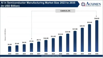
The global artificial intelligence in semiconductor manufacturing market size was valued at USD 6.50 billion in 2025 and is expected to reach USD 26.82 billion by 2035, while expanding at a CAGR of 15.2% during the forecast period of 2026-2035. Global semiconductor manufacturing capacity is projected to reach 11.1 million wafers per month by 2028, while capacity for advanced 7nm-and-below processes is expected to increase 69%, from 850,000 wafers/month in 2024 to 1.4 million in 2028, increasing the need for AI-enabled monitoring and process optimization. In 2025, worldwide semiconductor manufacturing equipment sales increased 15% to $135.1 billion, up from $117.1 billion in 2024, reflecting continued expansion of advanced logic, memory and AI-related manufacturing capacity.
Report highlights
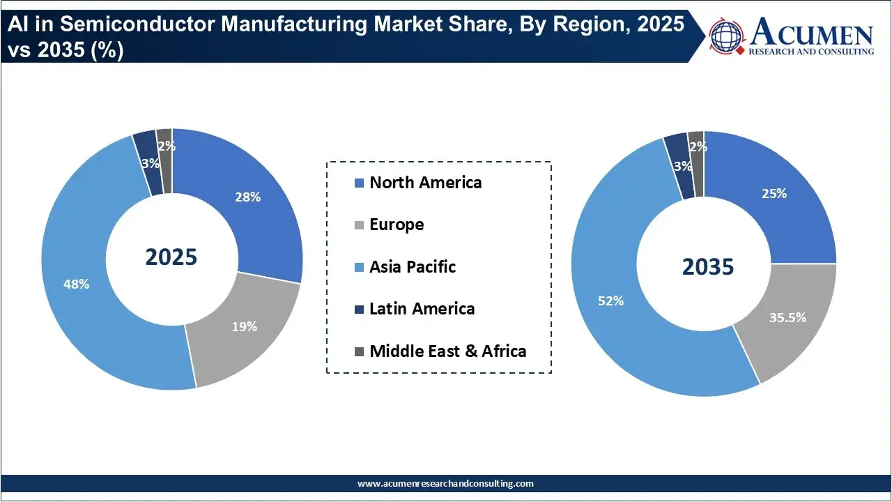
- By region, Asia Pacific dominated the market with a 48% share in 2025 and is projected to reach 52% by 2035, registering the highest regional CAGR of 16.2% from 2026 to 2035.
- By region, North America accounted for 28% of the market in 2025 and is projected to reach 25% by 2035, with the regional market expected to expand at a 13.7% CAGR from 2026 to 2035.
- By region, Latin America accounted for 3% of the market in 2025 and is projected to maintain a 3% share in 2035, with the regional market growing at a 15.2% CAGR from 2026 to 2035.
- By AI technology architecture, classical machine learning held the largest share of 48% in 2025, supported by its established use in fab analytics, equipment monitoring, process optimization and yield management.
- By AI technology architecture, deep learning held the second-largest share of 30% in 2025, driven by its growing application in wafer inspection, defect classification, anomaly detection and high-dimensional manufacturing data analysis.
- By offering, software / AI platforms dominated with a 46% share in 2025 and are projected to increase to 51% by 2035, reflecting rising demand for AI-driven analytics, process optimization and manufacturing intelligence.
- By deployment, on-premises / fab-local accounted for the largest share of 55% in 2025, supported by semiconductor manufacturers' requirements for low-latency processing, data security and protection of proprietary manufacturing information.
- By deployment, cloud is projected to be the fastest-growing segment, recording a 20.8% CAGR from 2026 to 2035, as semiconductor manufacturers increasingly adopt centralized AI training, analytics, predictive maintenance and cross-fab data management.
- By application, yield optimization & prediction held the largest share of 24% in 2025, as manufacturers increasingly use AI to identify yield-loss drivers across process, equipment, inspection and metrology data.
- By application, defect detection & classification represented the second-largest share of 22% in 2025, driven by increasing use of deep learning and computer vision to identify, classify and investigate wafer defects.
- By manufacturing stage, wafer fabrication / front-end manufacturing dominated with a 58% share in 2025, reflecting the high volume of process, equipment, inspection and metrology data generated across advanced fabrication steps.
- By manufacturing stage, wafer testing & metrology accounted for 15% in 2025, supported by increasing adoption of AI for automated measurement analysis, defect recognition and predictive process control.
- By end user, integrated device manufacturers (IDMs) held the largest share of 42% in 2025, benefiting from their control over extensive manufacturing operations and access to large historical datasets across fabrication, equipment and yield processes.
- By end user, pure-play foundries represented the second-largest share at 38% in 2025, supported by high-volume chip production and the financial importance of improving yield, equipment utilization and manufacturing efficiency.
How Is AI Changing Semiconductor Manufacturing?
AI is pulling manufacturing processes from a realm of reactive monitoring to ones that become increasingly data-driven, predictive, and perhaps, someday, fully autonomous. Artificial intelligence (AI) and machine learning software is increasingly used to combine equipment signals, inspection images, metrology data, and manufacturing execution (MES) system information to recognize deviations, diagnose sources of problems, predict likely failures, and advise specific correction in all steps involved in silicon manufacturing, such as litography, etching, deposition, clean, and so on.
- The SEMI 2026 edge AI applications program will bring a set of edge applications on process control, yield improvement, equipment collaboration, predictive maintenance, etc., whereas the work done at IBM research shows how AI may be leveraged for wafer level problem diagnosis and analysis or to diagnose production inefficiency.
This establishes an artificial-intelligence enabled continuous loop, in which production information feeds manufacturing intelligence for smarter, faster feedback for better production yield, efficiency in tool usage and better handling of the complexity required when pursuing advanced node logic or memory production.
AI Chip Demand and Semiconductor Manufacturing Capacity: Global Data & Statistics
- AI chip production increases demand for advanced packaging techniques such as 2.5D/3D packaging, chiplets and hybrid bonding and results in further investments outside traditional wafer manufacturing.
- Global capacity for advanced (7nm and below) processes is projected to grow by 69% from around 850,000 wafers per month in 2024 to about 1.4 million wafers per month by 2028.
- Overall, semiconductor equipment sales grew by 15% from $117.1B in 2024 to $135.1B in 2025 driven by significant investment into new fabs and production.
- The Chinese share in global semiconductor manufacturing capacity is anticipated to reach approximately 30% by 2030, driven by continued investments into local fabrication facilities.
- Taiwan is continuing to maintain leadership in advanced semiconductor manufacturing with TSMC expanding capacity for AI accelerators, HPC devices and advanced-node processors.
- TSMC has committed to investing $165B+ in the U.S., including additional fabs, advanced packaging capabilities and an R&D center in Arizona.
- South Korea has announced plans of around KRW 26T ($19B) in government incentives for its semiconductor industry to strengthen local manufacturing capacity and drive investment in AI-related chips.
- India has approved its first semiconductor fabrication project, a joint venture between Tata Electronics and Powerchip with an investment of around ₹91,000 crore, an important step toward establishing local chip manufacturing.
- The Indian government has cleared proposals worth more than 1.5 lakh crore in combined investment across semiconductor fabrication, packaging, testing and other related manufacturing.
- Japan is also promoting advanced chip manufacturing through initiatives like Rapidus (the government-backed company targeting 2nm-class chips).
- The surge in demand for HBM is causing Samsung, SK hynix and Micron to rapidly increase investment since AI accelerators demand much more memory bandwidth than conventional computers.
How Are Leading Semiconductor Companies Using AI?
| Company | How AI is being used |
|---|---|
| TSMC | TSMC is applying AI across computational lithography, advanced process control, defect inspection, process simulation and fab operations optimization; its collaboration with NVIDIA has also improved nanometer-scale defect inspection and reduced repeated labeling and retraining. |
| Samsung Electronics | Samsung is using AI for computational lithography, predictive maintenance, anomaly detection, logistics optimization and digital twins, with its planned AI factory supported by 50,000 NVIDIA GPUs. |
| Intel | Intel is applying machine learning to real-time defect analysis, process monitoring and advanced manufacturing, while expanding AI-focused foundry and advanced-node production capabilities. |
| Micron Technology | Micron is using AI-driven manufacturing and analytics to support memory production, process optimization and yield improvement, while expanding capacity to meet the growing demand for AI-related memory. |
| SK hynix | SK hynix is increasingly using AI and automation across HBM and advanced memory manufacturing, as AI accelerator demand drives the need for higher-yield and more efficient production. |
| ASML | ASML applies AI and machine learning to areas including equipment optimization, predictive maintenance and EUV manufacturing processes, helping improve equipment availability and production efficiency. |
| Applied Materials | Applied Materials uses AI and digital-twin technologies to optimize process control, equipment performance, fab layouts and semiconductor manufacturing workflows. NVIDIA identifies Applied Materials among companies using accelerated computing and AI for semiconductor manufacturing. |
| KLA | KLA is leveraging AI and machine learning in wafer inspection, metrology and defect classification, helping fabs identify increasingly small process defects and improve yield. |
| GlobalFoundries | GlobalFoundries is applying machine learning to advanced process control and semiconductor design workflows, supporting greater automation and process optimization. |
Market Dynamics
Driver
Rising AI Chip Demand and Advanced Fab Investment
The growth in demand for AI chips and investment in advanced fabs will expedite the use of AI in semiconductor fabrication. Global sales of semiconductor manufacturing equipment grew 15% to $135.1 billion in 2025; investment grew at logic and memory AI expansion and wafer capacity. Investment sales increased 90% to $31.5 billion in Taiwan and it became largest investor of Semiconductor Equipment on 2025, and sales increased 26% to $25.7 billion in Korea.
As it is known that manufacturing is more complex in 2025 than 2024, advanced fabs like TSMC and Samsung are bringing their AI investment directly in the fabs to conduct computational lithography, process simulation, defect inspection, predictive maintenance and process optimization.
As an instance, TSMC work with NVIDIA by implementing AI for lithography, advance process control, automated defect inspection by using NVIDIA's AI technologies and Samsung have achieved 20 performances improvement of computational lithography by using NVIDIA optimized architecture.
Restraint
High AI Implementation Costs and Data Integration Challenges
High implementation costs, data complexity and the difficulty of integrating AI into highly controlled semiconductor production environments can limit adoption. AI deployment often requires significant investment in computing infrastructure, sensors, inspection systems, software integration and high-quality manufacturing data, while fabs must validate AI outputs against strict process and quality requirements before allowing them to influence production decisions. The scale of semiconductor manufacturing investment also illustrates the financial barrier: global equipment spending reached $135.1 billion in 2025, with China alone accounting for $49.3 billion, Taiwan $31.5 billion and South Korea $25.7 billion.
Opportunity
Expansion of AI-Powered Process Control and Intelligent Fabs
Increased use of AI for automated process control, automated inspection and the intelligent fab opens opportunities for both AI technology providers and Semiconductor equipment vendors. The most attractive opportunity moving forward will be the shift away from discrete AI functions into integrated systems that weave together inspection, metrology, equipment and manufacturing data into continuous loops.
TSMC is already using AI for inspection for nanometer-scale defects and is implementing digital twin technologies for their fabs to enable predictive maintenance, optimize operations and control decisions in real-time. Growth in sophisticated packaging and testing continues to fuel the opportunity; global test equipment billings in 2025 increased 55% YOY and assembly and packaging equipment sales grew 21%, opening additional use-cases for AI based defect classification, yield optimization and process monitoring.
Regional Insights
What Made Asia Pacific the Largest Marketplace for AI Semiconductor Manufacturing?
Asia Pacific had a dominant share of 48% in 2025 which is expected to grow to 52% by 2035, becoming both the strongest and the highest growing regions at 16.2% CAGR. The region’s enormous semiconductor ecosystem centered across Taiwan, China, South Korea and Japan includes a full spectrum of foundries, IDMs, memory companies, device equipment makers, packaging specialists and electronic product manufacturing facilities.
High concentration of wafer manufacturing has an inherent output of an abundance of data pertaining to equipment, manufacturing, and inspections where the applicability of AI powered manufacturing analytics is substantial.
Increasing production for advanced nodes and complex package geometries drive complexities in processes which demands adoption for AI applications in defect control. The expanding capabilities in AI-chip and broader semiconductor supply chains within this region will push for need of AI which will help in increasing fab utilization and reduces scrap, downtimes and variations in processes.
AI Semiconductor Manufacturing in Taiwan: Trends & Analysis
- AI demand is driving Taiwan into even more advanced manufacturing processes, with TSMC lining up several rounds of 2nm fabs at Hsinchu and Kaohsiung and continuing investment into advanced packaging and the leading edge manufacturing infrastructure.
- AI based process control is a part of TSMCs day-to-day manufacturing processes, including intelligent detection, diagnosis, self learning, fault detection & classification, advanced equipment control and advanced process control.
- TSMC is introducing AI into fab scheduling and production equipment productivity, as AI is used within the dispatch system to optimize scheduling to increase equipment productivity.
- Advanced node manufacturing is becoming increasingly critical for Taiwan's AI semiconductor ecosystem, and TSMC already reported that 7 nm and beyond accounted for 74% of all wafer revenue in 2025, up from 69% in 2024.
- 3nm already represents a huge part of advanced semiconductor manufacturing, and accounted for 24% of all wafer revenue in 2025, increasing the need for precision AI supported process control and defect detection.
- Advanced packaging is becoming a manufacturing bottleneck for AI, and the Taiwanese ecosystem is increasingly focusing on CoWoS, InFO and SoIC as methods of fabricating high-performance AI processors.
North America to Boost with its Semiconductor Fab Investment by 2035
North America contributed around 28% in the year 2025, the market in North America is foreseen to grow from approximately $2.11billion to $6.71 billion with a CAGR of 13.7% from the year 2026 to the year 2035. North America is leading market for the AI-enhanced semiconductor manufacturing. This is due to the strong investments into wafer fab equipment, advance wafers fabs, AI infrastructure, domestic chips production capacities.
The advanced AI-aided IDMs, foundries, equipment providers and AI technology players are together augmenting the adoption of AI for the yield enhancement and defect detection and other machine learning applications like predicting maintenance and in the real-time controlling process data. Strong growth of AI chips the leading semiconductors for modern applications and building of American semiconductor manufacturing facilities are expected to spur the need of this demand for AI-driven fab automation in the forthcoming days.
Latin America to Grow Rapidly in AI Semiconductor Investments
The Latin America artificial intelligence in semiconductor manufacturing market is expected to grow at 15.2% CAGR between 2026 and 2035 on account of the growth in electronics manufacturing, semiconductor assembly and testing activities, rise in industrial automation and slow adoption of AI-based manufacturing solutions. Development of localized electronics and semiconductor supply chain in Latin American countries also presents ample opportunities for utilization of AI solutions in applications such as defect detection, predictive maintenance, process monitoring, quality control and process optimization.
While Latin American advanced semiconductor manufacturing landscape is not as strong as that in North America, Europe and Asia-Pacific yet with increasing manufacturing initiatives in domestic and developing countries and increase in digitalization in manufacturing sectors, AI is expected to grow with a rapid pace in Latin American semiconductor sector.
Segmental Insights
AI Technology Insight
The classical machine learning segment occupied the largest share of 48% in 2025 due to its widespread use throughout semiconductor manufacturing workflows. It is well suited to the structured fab data that are derived from equipment sensors, process parameters, wafer measurement and production records.
Additionally, given the somewhat established implementation ecosystem for classical machine learning models in the fab, it is relatively simpler to integrate them into the existing manufacturing execution systems and fab analytics platforms.
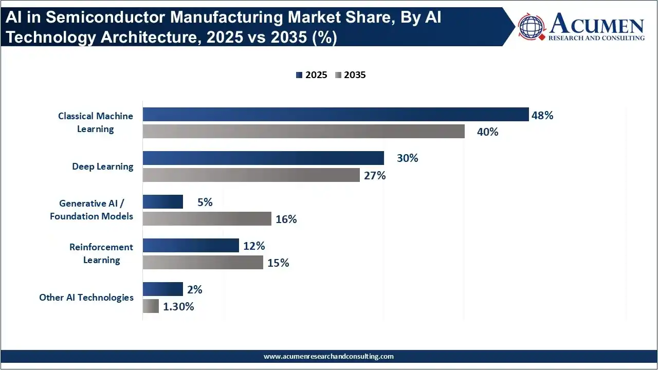
Deep learning commanded the second largest segment share of 30% in 2025 owing to its capacity to analyze complex high dimensional data structures commonly observed in semiconductor manufacturing. Deep learning models are well suited for equipment anomaly detection, pattern recognition, wafer inspection, and defect classification.
Its ability to identify subtle wafer defect patterns in wafer image sets and inspection data can help reduce manual review and improve classification. Deep learning is increasingly being used for advanced node manufacturing as more complex structures and tighter process margins require advanced solutions.
Offering Insights
Software/ AI platforms represented a 46% segment of the market in 2025, a share that will rise to 51% in 2035. The use of AI algorithms, analytics platforms, machine-learning models, and manufacturing intelligence software to glean actionable information from raw fab data is increasingly vital to manufacturers. The segment advantages software due to the ability to scale, for AI models can be constantly retrained and deployed in numerous manufacturing lines and facilities.
It will also grow as more organizations use cloud/hybrid architectures, artificial intelligence, and Machine Learning to optimize yield and control processes.
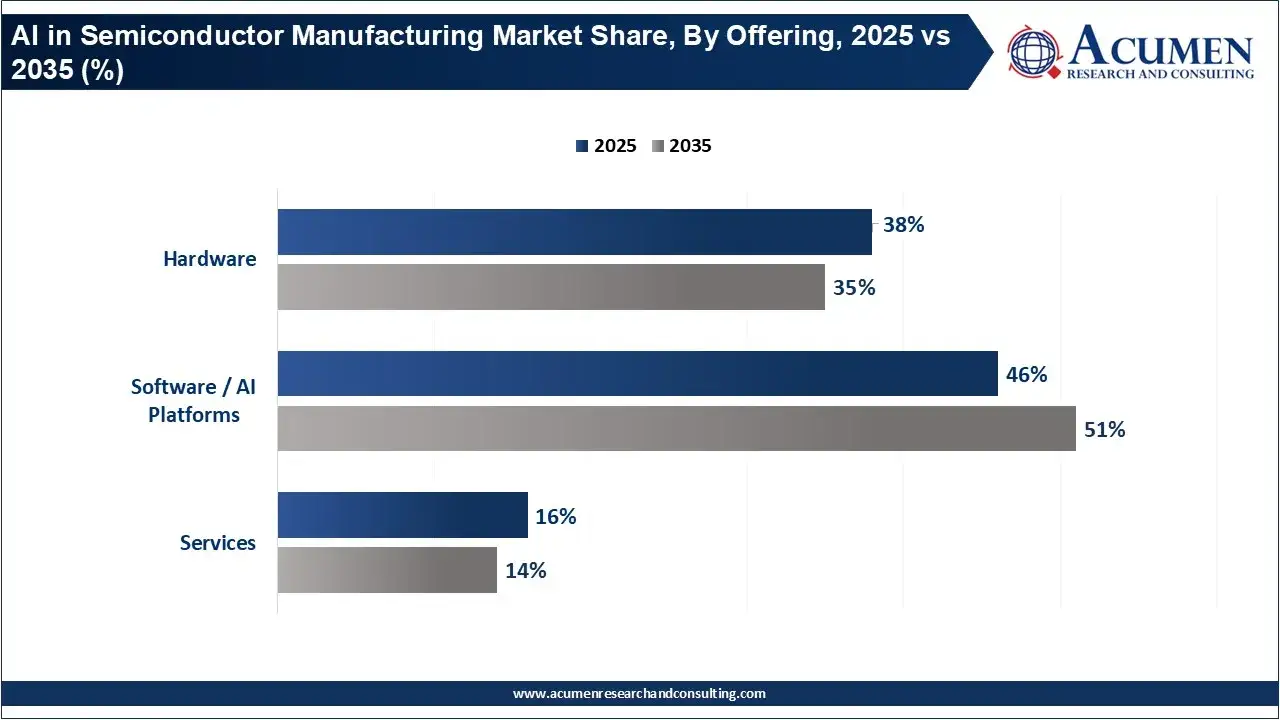
Hardware in 2025 represented a 38% segment of the market, making it the second largest segment. AI hardware includes computing infrastructure such as servers, AI-optimized chips, edge processing hardware and the specialized equipment needed for semiconductor manufacturing. Equipment continues to be important because any AI solution or algorithm is contingent on data generated by sensors, cameras and metrology instruments.
Deployment Insights
In 2025 on-premises captured a 55% share of the market. This high share reflected the semiconductor industry's unique demand for data security, latency, reliability of operations, and security of proprietary Intellectual Property. Semiconductor manufacturing facilities produce highly sensitive production data including recipes, equipment performance and yielding information and proprietary manufacturing processes.
AI in Semiconductor Manufacturing Market Share, By Deployment, 2025 & 2035 (%)
| Deployment | Revenue Share, 2025 (%) | Revenue Share, 2035 (%) |
|---|---|---|
| On-Premises / Fab-Local | 55% | 42% |
| Cloud | 15% | 23% |
| Hybrid | 30% | 35% |
Cloud deployment is the fastest-growing deployment segment, with a projected 20.8% CAGR from 2026 to 2035. Cloud adoption is particularly relevant for enterprise-level analytics, AI model training, benchmarking, supply-chain optimization and predictive maintenance. As semiconductor companies expand globally and operate increasingly interconnected manufacturing networks, the ability to centrally analyze production data is expected to accelerate cloud adoption.
Application Insights
Yield optimization and prediction constituted the largest market segment with a 24% share in 2025. Yield is one of the most critical financial performance metrics for manufacturing semiconductors. AI systems process past process parameters, wafer inspections, machine condition and metrology to identify variables impacting yield loss. This makes the application of AI to yield management very attractive as advanced semiconductor processing is becoming extremely sensitive to slight variations.
AI in Semiconductor Manufacturing Market Share, By Application, 2025 (%)
| Application | Revenue Share, 2025 (%) |
|---|---|
| Yield Optimization & Prediction | 24% |
| Defect Detection & Classification | 22% |
| Process Control & Optimization | 19% |
| Predictive Maintenance & Equipment Health | 17% |
| Manufacturing Planning & Scheduling | 8% |
| Supply Chain & Inventory Optimization | 7% |
| Others | 3% |
Defect detection and classification made up the second largest segment holding a 22% share in 2025. The application of AI to inspection systems could drastically reduce the time and effort required by human engineers to analyze and classify defects after wafer inspection. Deep learning and computer vision can distinguish between different defect types, identify recurring patterns and support root-cause investigations.
Manufacturing Insights
Wafer fabrication and front end manufacturing took the largest share at 58% in 2025 due to the clustering of AI applications in the front-end's most data-intensive and technically demanding production stage. Both front-end fabs process volumes of metrology, inspection, process and equipment data across multiple steps including deposition, lithography, etch, cleans etc.
Increasing economic benefits of yield improvements in wafer fab were also considered high as a front-end defect can propagate to many subsequent processing steps.
AI in Semiconductor Manufacturing Market Share, By Manufacturing Stage, 2025 (%)
| Manufacturing Stage | Revenue Share, 2025 (%) |
|---|---|
| Wafer Fabrication / Front-End Manufacturing | 58% |
| Wafer Testing & Metrology | 15% |
| Assembly & Packaging | 14% |
| Final Testing | 10% |
| Others | 3% |
Wafer testing and metrology constituted a 15% market share in 2025 with a growing market fueled by the drive for automated measurement, defect recognition and process confirmation. AI could correlate measurement patterns across wafers or lots and reveal trends that might be missed in routine measurement checks.
With integrated metrology with processing and equipment information, the market is moving beyond measurement towards predictive process control thus making AI of growing importance as precision becomes the key for advanced technology node manufacturing processes.
End User Insights
Integrated Device Manufacturers (IDMs), as the largest end user in 2025 represented 42% of market. IDMs have a significant role due to their broad ownership across wafer fabricating processes including design, production and at times testing, and deep access into the historic manufacturing data.
They carry processes necessary to leverage AI into all areas including yield management, equipment monitoring, defect inspection and process improvement. In large multi fab and production flow environments, they have many chances to ensure uniformity of AI technology across all plants/lines and different product streams.
AI in Semiconductor Manufacturing Market Share, By End User, 2025 (%)
| End User | Revenue Share, 2025 (%) |
|---|---|
| Integrated Device Manufacturers (IDMs) | 42% |
| Pure-Play Foundries | 38% |
| OSATs / Semiconductor Packaging & Testing Companies | 17% |
| Other Semiconductor Manufacturers | 3% |
Pure-play foundries made up 38% of the the market in 2025, reflecting their central role in manufacturing chips for fabless semiconductor companies. Foundries operate high-volume production environments where even small improvements in yield, throughput and equipment utilization can have significant financial implications.
Competitive Landscape
- TSMC: AI and accelerated computing are being applied by TSMC to its chip design and manufacture, including lithography, process simulation, defect inspection and fab operations.
- Samsung Electronics: Samsung is focused on building out its AI enabled manufacturing and developing a 50,000 strong NVIDIA GPU AI factory for state-of-the art chip manufacturing and smart factory operations.
- Intel: Intel is bringing AI and machine learning across its chip manufacturing processes and process optimization while growing its advanced-node and foundry capacities.
- NVIDIA: NVIDIA offers key AI computing infrastructure, its CUDA-X library of compute and visualization libraries and its digital twin technology for semiconductor lithography, inspection, process simulation and fab optimization.
- Applied Materials: Applied Materials is bringing in AI, analytics and digital twin technology to its semiconductor equipment and manufacturing processes where AI driven demand and capacity expansion is occurring.
- KLA Corporation: AI enables its inspection, metrology and process control platforms are being enhanced by its leading position in computing and AI for defect detection and chip manufacturing yield.
- Lam Research: Lam Research's intelligent process technology is being built up with respect to its etch and deposition equipment as factories require equipment data, process monitoring and AI enabled process optimization.
- ASML: ASML remains critical in the state-of-the art semiconductor manufacturing arena due to its EUV lithography equipment, and its role in AI and computation is increasing for the optimization of advanced lithography.
- Tokyo Electron: This is a major semiconductor equipment supplier whose process technology and data are increasingly important to AI driven processes and intelligent factories.
- Synopsys: AI and accelerated computing is being applied by Synopsys across its EDA, simulation and engineering workflows to bridge chip design and manufacturing optimization.
- Cadence Design Systems: Cadence is implementing AI and accelerated computing in its design, simulation and engineering workflow for advanced node manufacturing.
- Siemens: Siemens is involved in AI enabled semiconductors with industrial software and AI driven digital twin technology for manufacturing and fab optimization.
- Onto Innovation: This company focuses on inspection, metrology and process-control solutions enabling AI driven defect detection, process monitoring and yield optimization.
Recent News, Product Launches & M&A
- February 2026: Siemens acquired Canopus AI to strengthen its semiconductor manufacturing portfolio with AI- and machine-learning-based metrology and inspection, including technology for measuring edge placement error (EPE) to improve wafer-manufacturing simulation models.
- May 2026: Applied Materials and TSMC announced an innovation partnership at Applied Materials' $5 billion EPIC Center to accelerate semiconductor process technologies needed for the next generation of AI and high-performance computing.
Segments Covered
By AI Technology Architecture
- Classical Machine Learning
- Deep Learning
- Generative AI / Foundation Models
- Reinforcement Learning
- Other AI Technologies
By Offering
- Hardware
- Software / AI Platforms
- Services
By Deployment
- On-Premises / Fab-Local
- Cloud
- Hybrid
By Application
- Yield Optimization & Prediction
- Defect Detection & Classification
- Process Control & Optimization
- Predictive Maintenance & Equipment Health
- Manufacturing Planning & Scheduling
- Supply Chain & Inventory Optimization
- Others
By Manufacturing Stage
- Wafer Fabrication / Front-End Manufacturing
- Wafer Testing & Metrology
- Assembly & Packaging
- Final Testing
- Other
By End User
- Integrated Device Manufacturers (IDMs)
- Pure-Play Foundries
- OSATs / Semiconductor Packaging & Testing Companies
- Other Semiconductor Manufacturers
By Region
- North America
- Europe
- Asia Pacific
- Latin America
- Middle East & Africa (MEA)
Looking for discounts, bulk pricing, or custom solutions? Contact us today at sales@acumenresearchandconsulting.com
Frequently Asked Questions

Other Semiconductor and Electronics Reports
July 2024
July 2020
August 2026
June 2024