
Semiconductor Process Control Equipment Market Size, Share, Trends, Report 2026 To 2035
Semiconductor Process Control Equipment Market (By Equipment Type: Inspection Systems, Metrology Systems, Defect Review & Analysis Systems; By Technology: Optical-Based, Electron Beam-Based, X-Ray-Based, Scanning Probe / AFM-Based, Electrical / Sensor-Based, Other; By Wafer Size: 300 mm, 200 mm, ≤150 mm, Other; By End User: Pure-Play Foundries, IDMs, Memory Manufacturers, OSATs, Other; By Manufacturing Application: Front-End of the Line (FEOL), Middle-of-Line / MOL, Back-End-of-Line / BEOL, Advanced Packaging, Wafer-Level Testing, Final / Package Testing, Other; By Deployment Configuration: Inline / In-Situ, Standalone / Offline) - Global Industry Analysis, Size, Share, Regional Analysis, Trends and Forecast 2026 - 2035
- Last Updated: 17 Aug 2026
- Report Code: ARC3963
- Category: Semiconductor and Electronics
Semiconductor Process Control Equipment Market Size, Forecast 2026 To 2035
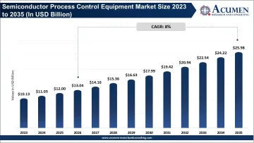
The global semiconductor process control equipment market size was valued at USD 12 billion in 2025 and is seen to reach at USD 25.98 billion by 2035 while growing at a promising CAGR of 8.0% during the forecast period of 2026-2035. The increasing complexity of advanced semiconductor nodes, including 3 nm, 2 nm and below, is driving demand for high-precision inspection, metrology and process control equipment as manufacturers face tighter process windows and greater sensitivity to defects and process variation. At the same time, rising investments in new fabs, advanced packaging and AI-chip manufacturing are increasing the need for real-time process monitoring, automated defect detection and data-driven yield optimization across semiconductor production lines.
Report Highlights
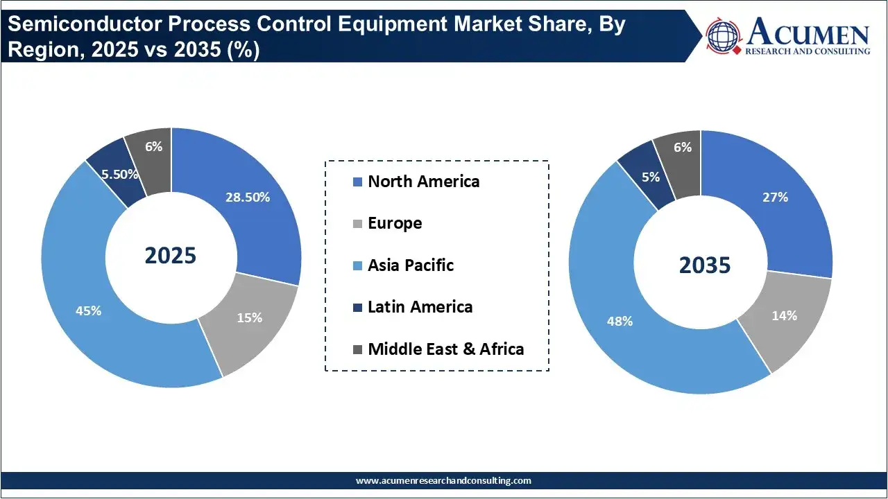
- By region, Asia Pacific dominated the market with a 45% share in 2025 and is projected to reach 48% by 2035, with regional revenue expected to grow from $5.87 billion in 2026 to $12.47 billion by 2035 at an 8.7% CAGR.
- By region, North America accounted for 28.5% of the market in 2025 and is projected to hold 27% by 2035, with the regional market expected to grow from $3.72 billion in 2026 to $7.01 billion by 2035 at a 7.3% CAGR.
- By region, Middle East & Africa accounted for 6% of the market in 2025 and is projected to maintain the same 6% share by 2035, with the regional market expected to expand at an 8.0% CAGR during 2026–2035.
- By equipment type, inspection systems dominated the semiconductor process control equipment market with a 60% share in 2025, reflecting their critical role in identifying wafer defects, contamination, pattern irregularities and process deviations.
- By equipment type, metrology systems held the second-largest share of 33% in 2025 and are gaining importance as advanced transistor architectures, 3D NAND and complex semiconductor packaging require increasingly precise dimensional and process measurements.
- By technology, optical-based systems held the largest share of 58% in 2025, supported by their high-throughput inspection capabilities and widespread use across high-volume semiconductor manufacturing environments.
- By technology, electron-beam-based systems represented the second-largest segment with a 29% share in 2025 and are projected to reach 34% by 2035, supported by demand for higher-resolution inspection of increasingly small defects and advanced device structures.
- By wafer size, 300 mm wafers accounted for the dominant 72% share in 2025 and are projected to reach 75% by 2035, supported by their importance in advanced logic, memory and high-performance semiconductor production.
- By end user, IDMs accounted for the second-largest share of 27% in 2025, supported by their extensive manufacturing operations across logic, memory, automotive and specialty semiconductor production.
- By end user, pure-play foundries represented the largest share of 38% in 2025, driven by high-volume manufacturing requirements and the need to maintain yield, process uniformity and equipment utilization across customer production programs.
- By manufacturing application, front-end of the line (FEOL) dominated with a 55% share in 2025, as deposition, lithography, etching, implantation and cleaning require continuous inspection and metrology to maintain tight process tolerances.
- By manufacturing application, back-end-of-the-line (BEOL) held the second-largest share of 17% in 2025, driven by the need to monitor interconnect dimensions, alignment and material integrity as chip architectures become increasingly complex.
- By deployment configuration, inline/in-situ systems led the market with a 62% share in 2025, reflecting growing demand for real-time process monitoring and rapid feedback directly within semiconductor production lines.
- By deployment configuration, inline/in-situ systems are projected to increase their share to 68% by 2035, as manufacturers increasingly integrate process control directly into automated fab workflows.
Semiconductor Process Control Equipment Market Overview
The semiconductor process control equipment market is benefiting from expanded semiconductor manufacturing investment overall, in particularly advanced logic, HBM and advanced packaging. Global semiconductor equipment billings were at all-time high of $135.1 billion in 2025, a 15% jump from $117.1 billion in 2024. Wafer processing equipment billings grew 12% and test equipment billings 55%, fueled by the growing need for inspection and testing for AI devices and HBM.
AI is having more of a reshaping effect on the mix of equipment being requested rather than simply increasing overall fab investment. The SEMI’s global projections for semiconductor equipment spending now stand around $145 billion in 2026 and $156 billion in 2027, with investments increasingly skewed towards leading-edge logic, HBM, DRAM, advanced packaging and technology node migration toward 2nm-class.
Semiconductor Manufacturing Equipment Spending Trends
- Wafer-processing equipment sales increased 12% in 2025, to indicate continuing investment in leading edge logic, memory capacity and AI-related semiconductor production.
- Test-equipment billings surged 55% in 2025, as a greater emphasis is placed on measurement, inspection and testing of more complex AI chip and HBM architectures.
- Assembly and packaging equipment sales increased 21% in 2025 due to increasing adoption of advanced packaging technologies for AI and high performance computing.
- China spent $49.3 billion on semiconductor equipment in 2025, remaining the largest equipment-spending market in the world, although spending grew slightly by 0.5% over 2024.
- Taiwan's semiconductor-equipment spending grew by a massive 90% year-over-year to $31.5 billion in 2025 driven by the expansion of AI and HPC capacity.
- South Korea spent $25.8 billion on semiconductor equipment, a 26% increase year-over-year, predominantly due to investments in HBM and DRAM production.
- Japanese semiconductor-equipment spending increased 22% year-over-year in 2025 due to continued investment in its domestic advanced node manufacturing capability.
- Intel increased the firms projected 2026 capital expenditure to $20 billion, from the previous $18 billion expectation, focused on new CPU requirements, custom chips and new manufacturing techniques including 18A and 14A processes.
- In August 2026 South Korea announced a fund of 5 trillion won ($3.52 billion) to support the domestic material, component and fabless semiconductor sector, as well as 5 trillion won in trade finance for export focused supplier firms.
- According to Deutsche Bank estimates cited by Reuters, Chinese semiconductor-equipment manufacturers are poised to take 25%-30% of Chinas projected $28 billion wafer-fabrication-equipment market in 2026, a figure which jumps to approaching 40% when lithography and metrology are stripped from the market.
Market Dynamics
Driver
How is AI increasing demand for semiconductor process control equipment?
The rapid expansion of AI accelerators, HBM and advanced logic is increasing the number of process steps, inspection points and manufacturing variables that fabs must control. Global semiconductor equipment billings reached $135.1 billion in 2025, while test equipment alone grew 55%, demonstrating how AI-related chip complexity is increasing the requirement for measurement, inspection and process verification.
For process-control suppliers, the opportunity extends beyond conventional defect inspection because advanced-node manufacturing requires increasingly precise control of critical dimensions, overlay, film thickness, pattern defects and process variability. The move toward 2nm-class production and increasingly complex GAA structures is therefore creating demand for higher-resolution metrology, e-beam inspection, optical inspection and increasingly automated feedback systems
Restraint
What is limiting semiconductor process control equipment adoption?
The primary barrier is the high cost and the technical sophistication required to operate sophisticated process-control tools like high-resolution inspection and metrology tools. Geopolitical developments also contribute to the instability. Chip producers see an emerging value proposition in alternative suppliers as access to cutting-edge U.S. equipment could be limited by the government's export controls regime;
Reuters reported in August 2026 that South Korea’s Samsung Electronics and SK Hynix planned to test Chinese etch equipment from AMEC Inc as a possible safeguard against those potential measures.
Opportunity
Where is the next major process-control opportunity?
The strongest opportunity is emerging from the combination of AI-driven manufacturing, advanced packaging, HBM and regional semiconductor localization. Advanced packaging equipment sales increased 21% in 2025, while test equipment billings jumped 55%, creating additional demand for inspection and metrology beyond traditional front-end wafer fabrication.
There is also a significant opportunity in emerging semiconductor manufacturing regions as governments subsidize domestic capacity. South Korea's new 5 trillion-won semiconductor fund, Intel's move toward more than $20 billion of 2026 capital expenditure, and continued fab investment across Asia and North America are examples of investment that can translate into new requirements for process monitoring, inspection, metrology and automated process-control infrastructure.
Regional Insights
How Did Asia Pacific Dominate the Semiconductor Process Control Equipment Market in 2025?
Asia-Pacific dominated the semiconductor process control equipment market with a 45% share in 2025 and is projected to increase its share to 48% by 2035, making it the largest regional market throughout the forecast period. The regional market is expected to increase from approximately $5.87 billion in 2026 to $12.47 billion by 2035, representing an 8.7% CAGR.
The reason for this particular emphasis on region is the region has the semiconductor manufacturing ecosystem with large volume foundries, memory suppliers, IDMs, process equipment manufacturers, electronics manufacturing and advanced packaging sites throughout Taiwan, Korea, China and Japan. This has resulted in large deployed base of automated inspection and metrology systems.
The concentration of semiconductor manufacturing also represents a huge market for process control because semiconductor manufacturers require wafer quality, critical dimension, overlay, defect and process variability checks constantly on their high-volume production lines.
Given the ongoing investment in the region toward new areas such as AI chip production, high-performance processing (HPC), memory chip creation, and in advanced packaging and advanced logic will likely insure a robust market for advanced process control solutions well into the future.
Top Asian Countries with Large Semiconductor Investment and Process Control Demand
| Country | Semiconductor investment & manufacturing significance | Process control equipment demand |
|---|---|---|
| China | China is one of the largest semiconductor equipment-investment markets globally. SEMI projected more than $100 billion in semiconductor manufacturing equipment spending during 2025–2027, driven by domestic capacity expansion and supply-chain localization. | Large-scale expansion of fabs creates sustained demand for inspection systems, metrology, defect review and process monitoring, particularly across mature-node, memory, power semiconductor and increasingly advanced-node production. |
| South Korea | South Korea is a major memory and semiconductor manufacturing hub. SEMI projected approximately $81 billion in semiconductor equipment spending during 2025–2027, while the country's semiconductor megaprojects involve more than $576 billion in planned investments from Samsung, SK Hynix, suppliers and local governments. | Strong investment in memory, advanced logic and next-generation fabs supports demand for high-resolution inspection, electron-beam systems, metrology and advanced process-control equipment. |
| Taiwan | Taiwan is a leading advanced-foundry manufacturing center, with SEMI projecting approximately $75 billion in semiconductor equipment spending during 2025–2027. | The concentration of advanced-node production makes Taiwan a major market for critical-dimension metrology, optical and electron-beam inspection, overlay measurement and automated process control. |
| Japan | Japan maintains a broad semiconductor ecosystem spanning equipment, materials, specialty semiconductors, sensors and manufacturing. A recent TSMC–Sony project in Kumamoto involves $4.69 billion in investment and is targeting volume production by 2029, adding to the country's semiconductor manufacturing base. | Demand is supported by new fab construction, image-sensor production, power semiconductors and specialty devices. Japan's strong domestic equipment ecosystem also creates opportunities for inspection. |
| India | India is rapidly developing its semiconductor manufacturing and packaging ecosystem. The government reported 12 approved manufacturing units with cumulative investment exceeding ₹1.64 lakh crore, including fabs and packaging facilities, as part of its semiconductor strategy. | New fabs and OSAT/ATMP facilities are creating an emerging market for inspection, metrology, testing and quality-control equipment. The government's support includes up to 50% fiscal support for semiconductor fab project costs, which can accelerate the build-out of process-control infrastructure. |
North America Semiconductor Process Control Equipment Opportunities & Trends
North America was 28.5% of the market in 2025. The region market is predicted to grow from an estimated $3.72B in 2026 to $7.01B in 2035, an estimated 7.3% CAGR.
The opportunities for the region are tied to the growth in domestic and specifically U.S.-based fab capacity build-out. The emergence of new fabs and the expansion of existing fabs can generate direct new capacity demand. The modernization of existing manufacturing assets will likely trigger replacement and upgrade buying cycles as old equipment is taken out of production.
The region has many of the main equipment suppliers and technology developers which generates a more developed process-control technology ecosystem, which is being accelerated by advanced process nodes and increased fab capacity, which should create opportunities.
Middle East & Africa’s Semiconductor Investment and Process Control Equipment Demand Statistics
The Middle East & Africa accounted for 6% of the semiconductor process control equipment market in 2025 and is projected to maintain the share by 2035. The regional market is expected to grow rapidly, representing an 8.0% CAGR.
While not focused on the manufacturing of semiconductors, there are longer term opportunities in the region for semiconductor-related activities such as manufacturing and testing as the region sees emerging investments in technology infrastructure, electronics manufacturing, data centers, and industrial digitalization.
Countries in MEA region are looking to establish technology intensive industries may be seen to develop a demand for semiconductor testing and packaging as well as accompanying process control infrastructure. As demand for digital infrastructure and HPC increases, a long term opportunity for semiconductor-related manufacturing can be said to arise for inspection and quality control equipment.
Segmental Insights
Equipment Type Insights
The inspection systems section controlled the majority of the 2025 market with a market share of 60% of that 2025. That is consistent as semiconductor inspection has consistently proven to be one of the most crucial process control steps used on a chip as it allows engineers to quickly identify contamination, particles, pattern irregularities, surface imperfections and many other deviations on the wafer.
As semiconductor process technologies march toward smaller lithographic patterns and extremely complex device geometries, the economic loss associated with a very small defect rate grows exponentially, driving demand for high resolution/high throughput inspection technologies.
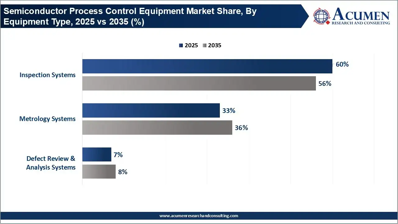
Metrology systems secured the second position in 2025 with a market share of 33%, and was driving growth due to their application as measurement of layer thickness, overlay, process control measurements and a broad range of parameters that will be required by smaller chip dimensions.
The development and adoption of advanced transistors, such as gate-all-around (GAA) as well as advanced and complex structures, such as 3D NAND and sophisticated packages will drive the segment as multiple measurements will be required, as well as critical and accurate control of multiple dimensions.
Technology Insights
The optical based technology segment accounted for the largest portion of the market 58% in 2025. These include established technologies utilized across many areas of wafer inspection and metrology since optical inspections provide high throughput wafer scan speeds that readily suit the high productivity of many fab operations.
Optical based inspection can continuously scan many square inches per minute, making them the process monitoring technology most favored by large production volume fabs that demand close, high-speed wafer monitoring.
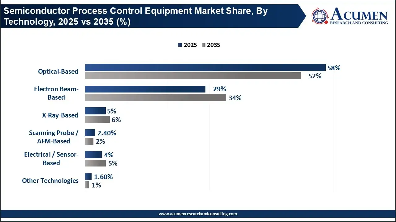
The second largest share was earned by electron-beam based technology 29% in 2025 and is predicted to increase its slice to 34% of the market by 2035. This growth comes in the midst of increasing semiconductor advances that require monitoring of ever smaller defects and features that the practical resolution of current optical inspection methods may now lack capabilities to monitor in wafer examination. Electron-beam offers these capabilities with respect to pattern inspection, defect review and monitoring of the smallest features used to build new integrated devices.
Wafer Size Insights
The 300 mm wafer segment dominated the market with a 72% share in 2025. This was due to high and advanced semiconductor manufacturing being increasingly focused on the 300 mm process node, as logic devices, memories and high performance computing continue to be pushed to their limits. The greater size of 300 mm wafers compared to other sizes allows for more dies to be cut out of each wafer, yielding greater profits while also favoring high value semiconductor types.
Semiconductor Process Control Equipment Market Share, By Wafer Size, 2025 & 2035 (%)
| Wafer Size | Revenue Share, 2025 (%) | Revenue Share, 2025 (%) |
|---|---|---|
| 300 mm | 72% | 75% |
| 200 mm | 22% | 20% |
| ≤150 mm | 4% | 3% |
| Other / Non-Wafer | 2% | 2% |
As the second largest market size category the 200 mm wafer segment controlled 22% of the market in 2025, its market importance is to be understood in mature and specialist application sectors including analog, power semiconductor, sensors, automotive application and industrial device segments. High volumes in these areas continue to necessitate a high manufacturing capacity while leading edge nodes dominate investments.
End User Insights
With a share of 38%, pure-play foundries stood at the forefront of the semiconductor process control equipment market in 2025. They have a larger market presence thanks to the scale of manufacturing on their own with and on behalf of various fabless semiconductor companies. Foundry facilities run large-scale production and their output is often gauged by equipment utilization, process uniformity and the optimum usage of yields.
Semiconductor Process Control Equipment Market Share, By End User, 2025 & 2035 (%)
| End User | Revenue Share, 2025 (%) |
|---|---|
| Pure-Play Foundries | 38% |
| IDMs | 27% |
| Memory Manufacturers | 25% |
| OSATs / Advanced Packaging & Testing | 8% |
| Other Semiconductor Manufacturers | 2% |
Integrated Device Manufacturer (IDM) were second behind pure-play foundry, with market share 27% in 2025. The integrated device maker was the second largest market as the IDM manages multiple stages in chip manufacturing, a fact which requires the use of process control equipment in several manufacturing stages.
Process control requirements range from upfront waiver fabrication to testing, with the occasional usage of packaging. These companies continue their significant contribution in the process control chip machinery market, partly thanks to substantial investment in manufacturing of the memory chips, logic chips, automotive chips and speciality devices by these makers.
Manufacturing Application Insights
The front-end of the line (FEOL) segment dominated the market with a 55% share in 2025. There are numerous highly sensitive stages in the FEOL manufacturing process such as, creation of transistors, deposition, etch, lithography and implantation/cleaning procedures. In line with number of individual stages and close tolerances in the FEOL process section, substantial requirements on continuous inspection and measurement are imposed.
Semiconductor Process Control Equipment Market Share, By Manufacturing Application, 2025 & 2035 (%)
| Manufacturing Application | Revenue Share, 2025 (%) |
|---|---|
| Front-End of the Line (FEOL) | 55% |
| Middle-of-Line / MOL | 8% |
| Back-End-of-Line / BEOL | 17% |
| Advanced Packaging | 10% |
| Wafer-Level Testing | 5% |
| Final / Package Testing | 4% |
| Others | 1% |
Back-end-of the line processing constituted the second most significant manufacturing application, taking 17% of total manufacturing applications in 2025. The BEOL processes produce those structures, such as interconnects, which tie the device together making it function correctly. They include several stages where dimensions, integrity of material and alignment of individual structures are of utmost important to assure high device performance.
Deployment Configuration Insights
Inline / in-situ deployment dominated the market with a 62% share in 2025 and is projected to increase to 68% by 2035. Its leadership reflects the semiconductor industry's preference for process monitoring that can be integrated directly into manufacturing workflows and provide rapid feedback during production.
Semiconductor Process Control Equipment Market Share, By Deployment, 2025 & 2035 (%)
| Deployment Configuration | Revenue Share, 2025 (%) | Revenue Share, 2035 (%) |
|---|---|---|
| Inline / In-Situ | 62% | 68% |
| Standalone / Offline | 38% | 32% |
Standalone / offline systems accounted for the second-largest share of 38% in 2025. These systems remain important for applications requiring detailed analysis, specialized measurements, laboratory-level characterization and additional defect review that may not be practical to perform directly within the production line.
Their role is particularly relevant for technology development, process qualification, failure analysis and advanced-node troubleshooting. While their share is projected to decline to 32% by 2035, they are expected to remain an important complementary component of semiconductor process-control infrastructure.
Leading Companies
- ASML Holding N.V. — ASML strengthens the process-control ecosystem through metrology and inspection technologies closely integrated with its advanced lithography platforms, particularly for overlay, critical-dimension and edge-placement control.
- Hitachi High-Tech Corporation — Hitachi High-Tech is particularly significant in electron-beam inspection and critical-dimension measurement, where high-resolution analysis is increasingly important for advanced semiconductor structures.
- Onto Innovation Inc. — Onto Innovation specializes in optical metrology, inspection and process-control solutions, with growing relevance in advanced packaging, wafer-level manufacturing and complex 3D semiconductor structures.
- Lasertec Corporation — Lasertec is an important inspection technology supplier, particularly in advanced semiconductor manufacturing where increasingly complex patterns and EUV-related processes require highly precise inspection and measurement capabilities.
- Nova Ltd. — Nova provides dimensional, materials and process-control metrology solutions that help fabs monitor critical process parameters and maintain tighter manufacturing tolerances as semiconductor geometries shrink.
- Tokyo Electron Limited (TEL) — TEL contributes to semiconductor process control through technologies integrated across wafer-processing workflows, supporting process monitoring and manufacturing optimization in high-volume fabs.
- Thermo Fisher Scientific Inc. — Thermo Fisher supports semiconductor process control through high-resolution electron microscopy and analytical technologies used for nanoscale defect analysis, materials characterization and failure investigation.
- Camtek Ltd. — Camtek provides inspection and metrology technologies with particular relevance to advanced packaging, including applications involving heterogeneous integration, high-density interconnects and complex package structures.
Recent News
- February 2026: Applied Materials introduced its Kinex, Centura Xtera, and PROVision 10 systems for advanced semiconductor manufacturing, with PROVision 10 offering 50% better imaging and 10× faster scanning, while Centura Xtera improves layer uniformity by 40% and reduces gas consumption by 50%.
- January 2026: KLA inaugurated a ₹300 crore R&D facility in Chennai spanning approximately 3.11 lakh sq. ft. and designed to accommodate up to 1,300 employees, strengthening its capabilities in semiconductor process control, software and AI.
Segments Covered
By Equipment Type
- Inspection Systems
- Metrology Systems
- Defect Review & Analysis Systems
By Technology
- Optical-Based
- Electron Beam-Based
- X-Ray-Based
- Scanning Probe / AFM-Based
- Electrical / Sensor-Based
- Other
By Wafer Size
- 300 mm
- 200 mm
- ≤150 mm
- Other / Non-Wafer
By End User
- Pure-Play Foundries
- IDMs
- Memory Manufacturers
- OSATs / Advanced Packaging & Testing
- Other Semiconductor Manufacturers
By Manufacturing Application
- Front-End of the Line (FEOL)
- Middle-of-Line / MOL
- Back-End-of-Line / BEOL
- Advanced Packaging
- Wafer-Level Testing
- Final / Package Testing
- Other
By Deployment Configuration
- Inline / In-Situ
- Standalone / Offline
By Region
- North America
- Europe
- Asia-Pacific
- Latin America
- Middle East & Africa
Looking for discounts, bulk pricing, or custom solutions? Contact us today at sales@acumenresearchandconsulting.com
Frequently Asked Questions

Other Semiconductor and Electronics Reports
May 2025
September 2024
December 2023
October 2024