
Digital Twin in Semiconductor Market Size, Share, Trends, Report 2026 To 2035
Digital Twin in Semiconductor Market (By Component: Software, Services; By Digital Twin Type: Product, Equipment/Asset, Process, Fab/System, Supply Chain; By Deployment Mode: On-Premises, Cloud, Hybrid; By Fab Type: Front-End, Back-End, Other; By End User: Foundries, IDMs, Fabless, OSAT, Equipment OEMs, EDA/Software, Research Institutes, Other) - Global Industry Analysis, Size, Share, Growth, Regional Analysis, Trends and Forecast 2026 - 2035
- Last Updated: 29 Aug 2026
- Report Code: ARC3971
- Category: Semiconductor and Electronics
Digital Twin in Semiconductor Market Size, Forecast Report 2026 To 2035
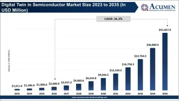
The global digital twin in semiconductor market size was valued at USD 1,900 million in 2025 and is projected to reach at USD 41,827 million by 2035; growing at a CAGR of 36.2% during the forecast period of 2026-2035. As semiconductor manufacturers expand AI, advanced logic, memory, advanced packaging, and high-performance computing production, the market is moving beyond static simulation toward connected, real-time, AI-enabled digital twins capable of supporting predictive and eventually autonomous manufacturing.
Report Highlights
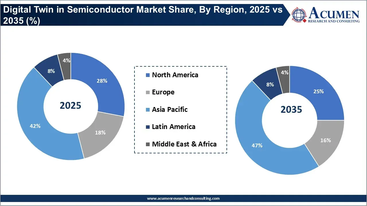
- By region, Asia-Pacific dominated the Digital Twin in Semiconductor Market in 2025 with a 42.0% share, supported by its concentration of semiconductor fabs, equipment manufacturers, advanced-node production, and large-scale manufacturing investments.
- By region, North America accounted for a 28.0% share in 2025, supported by its strong semiconductor design ecosystem, EDA industry, AI infrastructure, equipment manufacturers, and increasing domestic fab investments.
- By component, the software segment dominated the market in 2025 with a 72.0% share, supported by increasing demand for simulation, AI/ML analytics, data management, and semiconductor manufacturing integration.
- By component, the services segment is projected to grow at the fastest pace at a CAGR of 38.2% from 2026 to 2035, driven by rising requirements for system integration, digital-twin implementation, customization, cybersecurity, and ongoing technical support.
- By digital twin type, the process segment dominated the market in 2025 with a 48.0% share, owing to the need for process optimization, yield improvement, virtual experimentation, and real-time manufacturing control.
- By digital twin type, the product segment is expected to witness the fastest growth at a CAGR of 38.5% during 2026–2035, supported by increasing chip complexity, advanced packaging, AI accelerators, and lifecycle-based product monitoring.
- By deployment mode, the on-premises segment dominated the market in 2025 with a 42.0% share, primarily due to semiconductor manufacturers' requirements for greater control over sensitive production data, intellectual property, and fab operations.
- By deployment mode, the cloud segment held the second-largest share of 34.0% in 2025, supported by increasing demand for scalable computing, simulation, data storage, AI processing, and cross-facility digital-twin applications.
- By fab type, the front-end segment dominated the market in 2025 with a 72.0% share, driven by the extensive use of digital twins for wafer fabrication, process monitoring, equipment optimization, and yield management.
- By fab type, the back-end segment held the second-largest share of 23.0% in 2025, supported by increasing adoption of advanced packaging, 2.5D and 3D integration, thermal modeling, testing, and reliability analysis.
- By end user, the foundries segment dominated the market in 2025 with a 28.0% share, driven by high-volume manufacturing, complex production environments, equipment utilization requirements, and continuous yield optimization.
- By end user, the IDM segment held the second-largest share of 25.0% in 2025, supported by the integration of semiconductor design, manufacturing, product engineering, and lifecycle data within a single operating environment.
Digital Twin in Semiconductor Market Ecosystem
The digital twin semiconductor market ecosystem includes semiconductor fabricators, foundries and integrated device manufacturers (IDMs), fabless companies, equipment Original Equipment Manufacturers (OEMs), electronic design automation and simulation software suppliers, cloud computing and artificial intelligence (AI) technology companies, systems integrators, and academic research and educational institutions.
The digital twin ecosystem links physical chipmaking equipment, sensors, automated manufacturing execution systems, process-control solutions, metrology equipment, operational data, and supply-chain data to simulation, AI/ML, data analysis and digital twin solutions and technologies.
The trend is moving away from single digital twin devices and towards integrated process-line and entire-fab level environments to enable real-time analysis, proactive maintenance and prediction, what-if scenario planning, operational capacity optimization, increased semiconductor product yield and autonomous operations.
What Are the Major Applications of Digital Twins in Semiconductor Manufacturing?
- Process optimization: Simulates semiconductor manufacturing processes and evaluates process parameters, recipes, and operating conditions before physical implementation.
- Yield optimization: Correlates process, equipment, metrology, and product data to identify factors affecting wafer yield and accelerate yield learning.
Predictive maintenance: Uses equipment and sensor data to identify abnormal conditions and predict potential equipment failures before they cause unplanned downtime. - Equipment performance monitoring: Creates virtual representations of semiconductor tools to continuously monitor equipment health, performance, utilization, and operating conditions.
- Virtual commissioning: Allows manufacturers to test equipment configurations, production systems, automation, and factory processes digitally before physical deployment.
- Fab capacity planning: Simulates equipment availability, production capacity, WIP movement, and potential bottlenecks to improve long-term fab planning.
- Production scheduling: Uses real-time information from tools and WIP to optimize production schedules, maintenance timing, material movement, and line balancing.
- Defect detection and root-cause analysis: Combines inspection, process, and equipment information to identify anomalies and determine potential sources of defects.
Digital Twin in Semiconductor Market Economic Impact, Adoption and ROI Analysis
In 2025, global front-end semiconductor fab equipment spending is expected to increase by 8.9% to $110 billion and reach $130 billion in 2026, leading to a quickly growing installed base where tools can be more widely monitored, simulated, optimized for predictive maintenance and leveraged with digital twins.
The global semiconductor manufacturing capacity is forecast to grow to 11.1 million 300 mm wafer per month (wpm) by 2028 versus 10 million wpm in 2024, which makes it ever more important to establish the economics of fab capacity planning, optimization, yield improvement, and digital twins.
Growing use of advanced-node (<=7 nm) production will create a huge uplift in demand for digital process modeling: the capacity is expected to reach 1.4 million wpm in 2028, a 69% increase.
India has approved semiconductor projects including a Tata Electronics–PSMC fab designed for 50,000 wafers per month and multiple assembly and testing facilities with planned capacities ranging from 20,000 wafers per month to 96 million units per year, expanding the potential adoption base for digital manufacturing technologies.
In 2026, SMIC reported quarterly wafer shipments of 2.9 million 8-inch-equivalent wafers, up 14% sequentially, while utilization reached 93.7%, demonstrating how high utilization and capacity constraints increase the potential economic value of predictive maintenance and production optimization.
Market Dynamics
Driver
Rising Demand for AI-Driven Semiconductor Manufacturing
The exponential proliferation of AI, high performance computing, smart fabrication (fab) initiatives and advanced-node semiconductor manufacturing have increased the interest in digital twins throughout the semiconductor industry. Today’s manufacturing facilities feature extremely complex networks of equipment and processes.
Digital twins can be used to create a virtual model of a piece of equipment, manufacturing process, a production line or an entire fab.
They can then integrate the model with real-time data using AI and ML to predict yield, identify equipment issues, and experiment with production strategies in advance of implementing the changes on the factory floor.
Restraint
High Implementation Complexity and Data Integration Challenges
High implementation complexity, data-integration challenges, cybersecurity concerns, and the cost of developing high-fidelity models remain major restraints for the Digital Twin in Semiconductor Market. Semiconductor fabs generate enormous volumes of equipment, sensor, process, metrology, and production data, but these datasets can differ in format, quality, granularity, and frequency.
Connecting legacy equipment and multiple manufacturing systems into a synchronized digital-twin environment can therefore require substantial engineering and integration work. SEMI highlights unclean factory data, varying data granularity, data provenance, interoperability, and legacy equipment as key implementation challenges.
Opportunity
Growing Shift Toward Autonomous and Smart Semiconductor Fabs
The transition toward AI-driven and autonomous semiconductor fabs presents a major opportunity for digital-twin providers, semiconductor manufacturers, equipment OEMs, and technology companies. The opportunity is expanding from individual equipment monitoring toward interconnected digital twins covering processes, tools, products, facilities, and entire production systems. Such systems can support virtual commissioning, predictive maintenance, yield optimization, production scheduling, capacity planning, energy management, and advanced process control. Recent research on plasma etching demonstrates the potential of combining physics-based simulation with AI to create more data-efficient digital twins and reduce the number of physical experimental runs required for recipe development.
Segmentation Insights
Component Insights
The software segment dominated the digital twin in semiconductor market in 2025, accounting for 72.0% of the market, because semiconductor digital twins are highly technology intensive systems requiring platforms for simulation, modeling engines, algorithms powered by Artificial Intelligence/Machine Learning (AI/ML), platforms for data management. Moreover, the software as component is critical in industrial IoT connectivity, analytics, and integration capabilities to create and maintain virtual representations of semiconductor products, equipment, processes, and fabs.
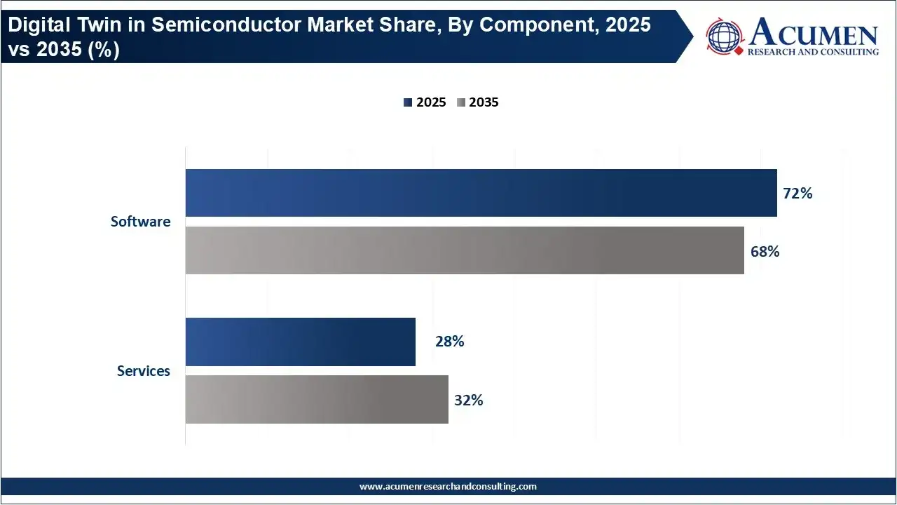
The services segment is expected to register the fastest growth, with its market share increasing from 28.0% in 2025 to 32.0% by 2035. The segment is projected to increase from $532.0 million in 2025 to $728.3 million in 2026 and reach approximately $13,384.6 million by 2035, representing a CAGR of 38.2%. The faster growth of services reflects the complexity involved in implementing digital twins across semiconductor fabs. Manufacturers often require consulting, system integration, data engineering, model development, customization, implementation, training, cybersecurity, maintenance, and ongoing optimization.
Digital Twin Type Insights
Process digital twin segment captured the major revenue share of 48.0%. The dominant position of the process digital twin segment is largely owing to the critical role of process optimization, improvement of yield, minimization of defects, management of process-window, virtual experimentation, and real-time process control in the manufacture of semiconductors.
Hundreds of processing steps involving careful control and accuracy across a spectrum of applications such as lithography, etching, deposition, temperature, pressure, and process parameters within the semiconductor manufacturing process where any slight change can have a cascading effect on the wafer yield. Process digital twin help the manufacturers simulate these conditions before physical testing the variables.
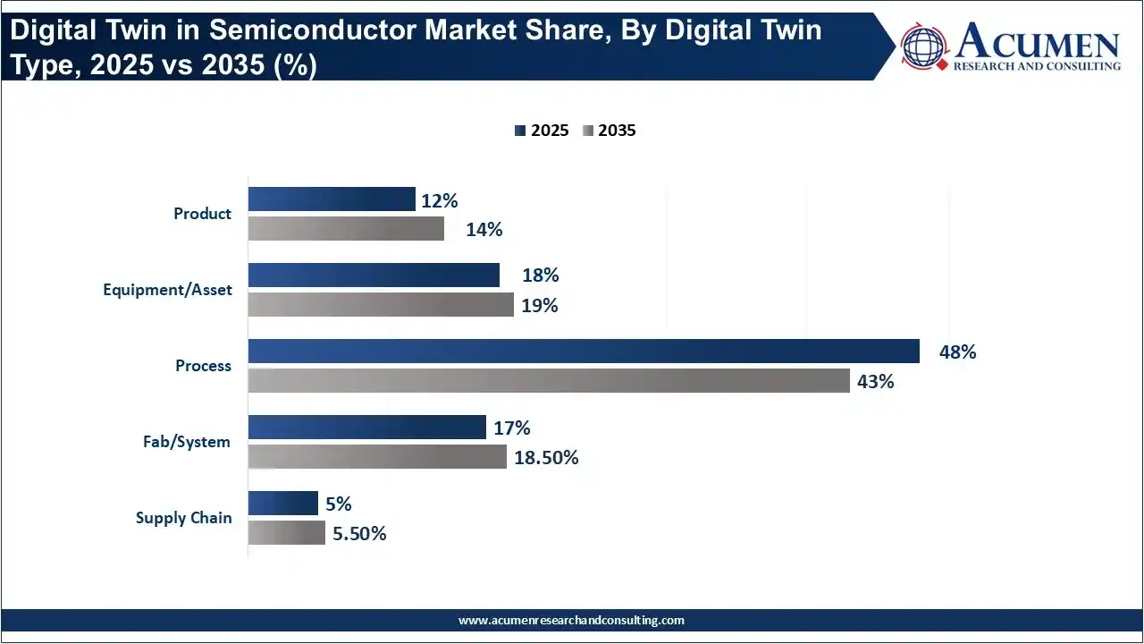
The product digital twin segment accounted for 12.0% in 2025 but is expected to register the fastest growth, reaching approximately $5,855.8 million by 2035 from $312.1 million in 2026, representing a CAGR of 38.5%. Product twins can connect semiconductor product characteristics with design, manufacturing, performance, reliability, and lifecycle data. Their growth is supported by increasingly complex chips, advanced packaging, heterogeneous integration, AI accelerators, high-performance computing, and the need to understand product behavior across the complete lifecycle.
Deployment Mode Insights
The on-premises segment accounted for a market share of 42.0%, followed by the cloud deployment segment. The on-premises deployment modality is key owing to the use of sensitive process data, information on proprietary manufacturing, equipment data, intellectual property (IP), information regarding advanced-node manufacturing being in the possession of semiconductor manufacturers.
Data security, system performance, data access and incorporation into the existing manufacturing systems are effectively controlled by managing the infrastructure in fab or the corporate infrastructure.
Digital Twin in Semiconductor Market Share, By Deployment Mode, 2025 (%)
| Deployment Mode | Revenue Share, 2025 (%) |
|---|---|
| On-Premises | 42% |
| Cloud | 34% |
| Hybrid | 24% |
The cloud deployment segment emerged to be the second-largest deployment modality by contributing to a market share of 34.0% in 2025. The digital twin technology requires significant computing resources such as that needed for simulation, analytics, computation intensive artificial intelligence and machine learning algorithm applications, data storage and for various kinds of modeling and scenario-building, thus making the cloud deployment of the digital twin a key component.
Fab Type Insights
The front-end segment dominated the market in 2025, accounting for 72.0% of the market. Front-end semiconductor manufacturing involves wafer fabrication processes such as lithography, deposition, etching, ion implantation, cleaning, chemical mechanical planarization, metrology, and inspection. These processes require extremely precise control and generate substantial amounts of equipment and process data, creating strong demand for digital twins.
The dominance of front-end fabs is also associated with the increasing complexity of advanced semiconductor nodes. As manufacturers move toward 3-nanometer, 2-nanometer, GAA, advanced memory, and other complex architectures, the need for virtual process experimentation, predictive process control, equipment simulation, defect analysis, and yield optimization increases.
Digital Twin in Semiconductor Market Share, By Fab Type, 2025 (%)
| Fab Type | Revenue Share, 2025 (%) |
|---|---|
| Front-End | 72% |
| Back-End | 23% |
| Other | 5% |
The back-end segment was the second-largest segment in 2025, accounting for 23%. Back-end applications include assembly, packaging, testing, and increasingly advanced packaging technologies such as 2.5D and 3D integration. Digital twins can support package design, thermal modeling, mechanical-stress analysis, assembly optimization, testing, reliability prediction, and advanced packaging process development. The importance of this segment is increasing alongside AI and high-performance computing because advanced processors increasingly depend on high-bandwidth memory, chiplets, 2.5D/3D packaging, and heterogeneous integration.
End User Insights
Based on the end users, in 2025 the foundries segment was the largest in the market with a share of 28.0% of the market. Foundries process a high volume, large-scale complex facility with significant needs around process optimization, equipment utilization, yield management, capacity planning and fab automation. The digital twin enables foundries to simulate production runs, optimize tool allocation, conduct fab layout analysis, predict tool failures and detect potential process deviations prior to their impact on a substantial production volume.
Digital Twin in Semiconductor Market Share, By End User, 2025 (%)
| End User | Revenue Share, 2025 (%) |
|---|---|
| Foundries | 28% |
| IDMs | 25% |
| Fabless | 12% |
| OSAT | 8% |
| Equipment OEMs | 15% |
| EDA/Software | 6% |
| Research Institutes | 4% |
| Other | 2% |
The next largest end-user segment for digital twins in semiconductor in 2025 was the IDM segment that contributed 25.0% to the overall market. Integrated device manufacturers combine semiconductor design capabilities with semiconductor manufacturing operations. This integration of design data and manufacturing, allows digital twins to link design details with manufacturing results, enable design-for-manufacturing, support process development, yield optimization, equipment, and product monitoring throughout a product’s lifecycle.
IDMs are investing more on new advanced manufacturing capacity including for high power discrete, automotive, memory and automotive semiconductor manufacturing, all of which benefit from digital twin technology.
Regional Insights
What Made Asia Pacific Dominate the Digital Twin in Semiconductor Market in 2025?
The Asia Pacific was accounted for 42.0% of the digital twin in semiconductor market in 2025, representing the biggest regional market and also it was the highest growing market in provided forecast. In 2025, the regional market size was about $798.0 million, it grew to $1,092.4 million in 2026 and is projected to reach about $19,658.7 million in 2035 growing at a CAGR of 37.9%. The leading position of the Asia-Pacific is attributed mainly to the significant concentration of wafer manufacturing in the region.
Taiwan is particularly important to the regional digital twin market because of its concentration of advanced foundry manufacturing. TSMC reported that its manufacturing facilities and subsidiaries exceeded 17 million 12-inch equivalent wafers of annual capacity in 2025, with major facilities across Taiwan and expanding operations in the United States and Japan. TSMC is also actively exploring FabTwin technology using NVIDIA Omniverse for virtual fab environments, including tool-layout evaluation and simulation workflows.
North America Digital Twin in Semiconductor Market Analysis:
Based on our research at Acumen Research & Consulting, North America was the second largest marketplace, holding a share of 28.0% in 2025. Valued at about $532.0 million in 2025 it grew to $728.3 million in 2026 and is expected to reach about $10,456.7 million by 2035, representing a CAGR of 34.5% during the 2026-2035 forecast period. This region's dominant position is reinforced by its semiconductor design community and simulation software market. Another responsible factors are AI community, semiconductor equipment manufacturers and also governmental support for domestic semiconductor manufacturing.
In North America the leading country is U.S. the increased usage of digital twins has started to link to increased development in U.S. based manufacturing facilities and intelligent factories that can use artificial intelligence. NVIDIA stated that they are helping TSMC utilize their omniverse solution with it facilitating and accelerating fab design and construction at their Arizona facility and across all other sectors of the U.S. manufacturing communities, factories that utilize factory-scale digital twins that support planning and manufacturing.
Government Initiatives and Policies
- United States: The CHIPS for America program announced up to $285 million in funding for a Manufacturing USA institute focused on digital twins for semiconductor manufacturing, advanced packaging, assembly, and testing.
- Taiwan: Taiwan is supporting digital twins through smart manufacturing programs integrating AI, robotics, edge computing, and digital-twin technologies, while strengthening semiconductor R&D and manufacturing under its strategic industry initiatives.
- South Korea: Government semiconductor and smart-factory programs are promoting AI, automation, digital manufacturing, and simulation across advanced semiconductor fabs, supporting applications such as predictive maintenance and process optimization.
- China: China's smart manufacturing policies encourage the integration of AI, IoT, industrial software, simulation, and digital twins into semiconductor production as the country expands domestic fab and equipment capabilities.
- European Union: The EU Chips Act supports semiconductor R&D, pilot lines, advanced manufacturing, packaging, and testing. The Chips for Europe Initiative provides up to €3.3 billion in EU funding, creating opportunities for digital-twin adoption.
Future Technology Roadmap
| Time Span | Technology Development | Key Industry Applications |
|---|---|---|
| 2026–2027 | AI-enabled equipment digital twins | Equipment health monitoring, predictive maintenance, anomaly detection, virtual commissioning |
| 2027–2028 | Real-time process digital twins | Virtual metrology, process-window optimization, recipe optimization, yield prediction |
| 2028–2029 | Multi-equipment and production-line twins | WIP tracking, production scheduling, bottleneck identification, line balancing |
| 2029–2030 | Fab-level digital twins | Complete fab simulation, capacity planning, layout optimization, what-if analysis |
| 2030–2031 | Physics-informed AI digital twins | Combining physics models with AI/ML for process and equipment prediction |
| 2031–2032 | Cloud-edge digital twin infrastructure | Edge processing, cloud simulation, federated data sharing, cross-fab analytics |
Key Companies
- NVIDIA Corporation
- Siemens AG
- Synopsys, Inc.
- Ansys, Inc.
- Cadence Design Systems, Inc.
- Dassault Systèmes SE
- PTC Inc.
- Schneider Electric SE
- Rockwell Automation, Inc.
- Autodesk, Inc.
- IBM Corporation
- Microsoft Corporation
- Applied Materials, Inc.
- Lam Research Corporation
Strategic Partnerships, Product Launches and Developments
- October 2025: NVIDIA and Samsung announced plans to build an AI factory using more than 50,000 NVIDIA GPUs, with Samsung developing digital twins of its global semiconductor fabs using NVIDIA Omniverse. The digital twins are intended to support predictive maintenance, real-time decision-making, logistics optimization, and factory automation. The collaboration also achieved 20x performance gains in computational lithography and TCAD simulations.
- October 2025: Siemens and NVIDIA showcased an advanced digital twin technology stack integrating Siemens Xcelerator with NVIDIA Omniverse. The solution is designed to combine 3D visualization, simulation, and factory data to create highly realistic digital twins for advanced manufacturing environments. For semiconductor manufacturers, the technology can simulate factory layouts, production lines, and operational scenarios before physical changes are implemented.
Segments Covered
By Component
- Software
- Services
By Digital Twin Type
- Product
- Equipment/Asset
- Process
- Fab/System
- Supply Chain
By Deployment Mode
- On-Premises
- Cloud
- Hybrid
By Fab Type
- Front-End
- Back-End
- Other
By End User
- Foundries
- IDMs
- Fabless
- OSAT
- Equipment OEMs
- EDA/Software
- Research Institutes
- Other
By Region
- North America
- Europe
- Asia-Pacific
- Latin America
- Middle East & Africa
Looking for discounts, bulk pricing, or custom solutions? Contact us today at sales@acumenresearchandconsulting.com
Frequently Asked Questions

Other Semiconductor and Electronics Reports
October 2023
July 2020
June 2021
February 2020