
Advanced Hybrid Bonding Equipment Market Size, Share, Trends, Report 2026 To 2035
Advanced Hybrid Bonding Equipment Market (By Bonding Approach: Wafer-to-Wafer (W2W), Die-to-Wafer (D2W), Die-to-Die & Collective Die-to-Wafer; By Equipment Type: Hybrid Bonding Systems, Surface Preparation & Activation, Alignment, Metrology & Inspection, Die Preparation & Handling; By Application: Logic & 3D SoC / Chiplets, 3D NAND, CMOS Image Sensors, HBM & DRAM, Others; By Interconnect Pitch: >=5 um pitch, 1 to <5 um pitch, <1 um pitch; By End User; IDMs & memory manufacturers, Foundries, OSATs, Research institutes & others; By Wafer Size; 300 mm, 200 mm & below) - Global Industry Analysis, Size, Share, Regional Analysis, Trends and Forecast 2026 - 2035
- Last Updated: 09 Nov 2026
- Report Code: ARC4004
- Category: Semiconductor and Electronics
Advanced Hybrid Bonding Equipment Market Size, Forecast Report 2026 To 2035
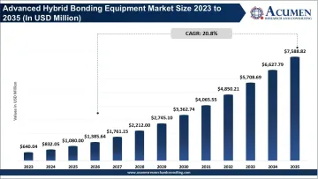
The global advanced hybrid bonding equipment market size was valued at $1,080 million in 2025 and is expected to surpass $7,588.82 million by 2035; expanding at a CAGR of 20.8% during the forecast period of 2026-2035. The advanced hybrid bonding equipment market is driven by increasing demand for high-bandwidth memory, 3D semiconductor integration, chiplet architectures, and advanced packaging. Growing investments in AI processors, high-performance computing, and next-generation memory manufacturing are further accelerating equipment adoption.
Advanced Hybrid Bonding Equipment Market Size & Forecast
- Base Year Market Size (2025): $1,080 million
- Current Year Market Size (2026): $1,385.64 million
- Estimated Year Market Size (2035): $7,588.82 million
- Forecast Period CAGR (2026-2035): 20.8%
Key Takeaways
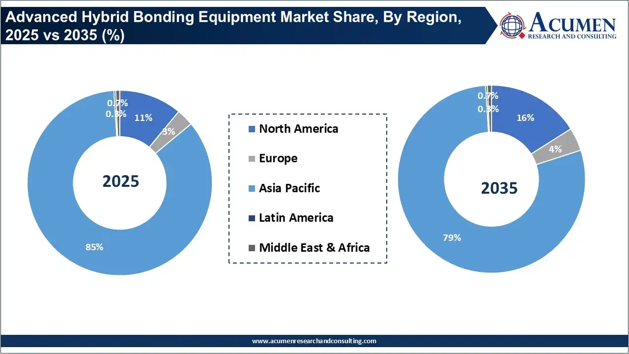
- By region: Asia-Pacific dominated the Advanced Hybrid Bonding Equipment Market with an 85.0% share in 2025, generating USD 918.00 million in revenue. The regional market is projected to reach USD 5,995.17 million by 2035, registering a 19.9% CAGR from 2026 to 2035.
- By bonding approach: Wafer-to-wafer (W2W) bonding dominated the market with a 56.0% share in 2025, generating USD 604.80 million in revenue. Die-to-wafer (D2W) bonding ranked second with a 42.0% share.
- By equipment type: Hybrid bonding systems dominated the equipment segment with a 62.0% share in 2025, generating USD 669.60 million in revenue. Surface preparation and activation equipment ranked second with an 18.0% share.
- By application: Logic and 3D SoC/chiplet applications dominated the market with a 38.0% share in 2025, generating USD 410.40 million in revenue. 3D NAND ranked second with a 30.0% share.
- By interconnect pitch: The 1 to less than 5 µm category dominated the market with a 50.0% share in 2025, generating USD 540.00 million in revenue. Interconnect pitches of at least 5 µm ranked second with a 38.0% share.
- By end user: IDMs and memory manufacturers dominated the end-user segment with a 58.0% share in 2025, generating USD 626.40 million in revenue. Foundries ranked second with a 33.0% share.
- By wafer size: The 300 mm wafer category dominated the market with a 92.0% share in 2025, generating USD 993.60 million in revenue. Wafers measuring 200 mm and below accounted for the remaining 8.0% share.
Advanced Hybrid Bonding Equipment Market Overview
The advanced hybrid bonding equipment market is gaining momentum as semiconductor manufacturers increasingly adopt advanced packaging technologies to improve interconnect density, performance, and power efficiency. Hybrid bonding enables direct copper-to-copper and dielectric-to-dielectric connections between semiconductor wafers or dies, reducing reliance on conventional solder micro-bumps and supporting finer-pitch interconnections. The technology is becoming increasingly important in high-bandwidth memory (HBM), 3D integrated circuits, chiplet-based architectures, advanced logic devices, and heterogeneous integration.
Growing demand for AI accelerators, high-performance computing, and next-generation semiconductor devices is encouraging foundries, integrated device manufacturers (IDMs), and outsourced semiconductor assembly and test (OSAT) providers to invest in specialized bonding systems. Equipment demand is also supported by advancements in wafer alignment, surface preparation, plasma activation, precision bonding, and post-bond inspection technologies.
Technology Landscape
| Technology | Description | Major applications |
|---|---|---|
| Wafer-to-Wafer (W2W) Hybrid Bonding | Bonds two semiconductor wafers through direct copper-to-copper and dielectric-to-dielectric interfaces. | 3D NAND, image sensors, memory stacking, and 3D integration. |
| Die-to-Wafer (D2W) Hybrid Bonding | Integrates individual semiconductor dies onto a target wafer using high-precision alignment and direct bonding. | HBM, chiplets, AI processors, and heterogeneous integration. |
| Die-to-Die (D2D) Hybrid Bonding | Connects individual semiconductor dies directly to achieve high-density electrical interconnections. | Advanced logic integration, chiplet architectures, and high-performance computing. |
| Copper-to-Copper (Cu-Cu) Bonding | Establishes direct electrical connections between copper interconnects without conventional solder bumps. | HBM, 3D ICs, and advanced semiconductor packaging. |
| Dielectric-to-Dielectric Bonding | Creates direct insulating-layer connections between semiconductor surfaces to establish mechanical bonding interfaces. | Wafer stacking, heterogeneous integration, and 3D semiconductor devices. |
| Plasma-Activated Bonding | Uses plasma treatment to improve surface energy and enable reliable bonding at lower processing temperatures. | Wafer-level packaging and advanced 3D integration. |
Equipment Ecosystem and Value Chain
- Semiconductor Hybrid Bonding Equipment Manufacturers: Develop and supply specialized bonding platforms designed for wafer-to-wafer, die-to-wafer, and die-to-die integration, supporting high-precision alignment and direct interconnect formation.
- Surface Preparation and Cleaning Equipment Providers: Supply systems for wafer cleaning, contamination removal, surface conditioning, and preparation to achieve defect-free bonding interfaces.
- Plasma Activation Equipment Manufacturers: Develop plasma treatment systems that modify wafer surface properties, improve surface energy, and facilitate reliable dielectric bonding.
- Precision Alignment and Positioning System Suppliers: Provide optical alignment, wafer positioning, die placement, and overlay control technologies required for accurate copper interconnection.
- Thermal Processing Equipment Manufacturers: Develop annealing and temperature-control systems that support copper-to-copper interface formation and improve bonding reliability.
- Integrated Device Manufacturers (IDMs): Invest in hybrid bonding capabilities to improve memory stacking, device integration, and semiconductor manufacturing performance.
Advanced Hybrid Bonding Equipment Market Dynamics
Growth Drivers
- Increasing Demand for Advanced Semiconductor Packaging: Growing demand for high-performance semiconductor devices is accelerating the adoption of advanced packaging technologies, including hybrid bonding. The technology enables finer interconnect pitches, higher interconnection density, and improved electrical performance compared with conventional microbump bonding, making it increasingly important for next-generation semiconductor integration.
- Growing Adoption of 3D NAND and HBM Technologies: Rising demand for high-bandwidth memory (HBM), advanced DRAM architectures, and vertically stacked 3D NAND is driving investments in hybrid bonding equipment. Semiconductor manufacturers are adopting hybrid bonding to achieve higher interconnect density, reduce connection distances, and improve bandwidth and power efficiency in memory-intensive applications.
Increasing Chiplet Integration and Heterogeneous Packaging: The growing use of chiplet architectures and heterogeneous integration is creating demand for precise wafer-to-wafer and die-to-wafer bonding equipment. Hybrid bonding enables the integration of different semiconductor dies with high-density interconnections, supporting advanced processors, AI accelerators, and high-performance computing applications.
Restraints
- High Equipment Acquisition and Installation Costs: Advanced hybrid bonding systems require sophisticated wafer alignment, surface preparation, cleaning, bonding, and inspection capabilities. The substantial capital investment associated with equipment procurement, facility preparation, and process integration can restrict adoption among smaller semiconductor manufacturers and packaging service providers.
- Complex Manufacturing and Process Requirements: Hybrid bonding requires extremely smooth, clean, and accurately aligned bonding surfaces to achieve reliable copper-to-copper and dielectric-to-dielectric connections. Maintaining precise surface flatness, contamination control, overlay accuracy, and bonding conditions increases process complexity and creates challenges for consistent high-volume production.
- Limited Standardization Across Manufacturing Processes: Differences in wafer dimensions, die architectures, materials, bonding configurations, and fabrication requirements can complicate equipment standardization. Equipment manufacturers must customize systems for specific semiconductor applications, increasing qualification timelines, integration requirements, and development costs.
Key Opportunities
- Expansion of AI and High-Performance Computing Infrastructure: Rapid growth in artificial intelligence, data centers, generative AI, and high-performance computing is creating opportunities for advanced hybrid bonding equipment. Increasing demand for high-bandwidth memory, advanced processors, and AI accelerators is encouraging semiconductor manufacturers to invest in high-density interconnection technologies and next-generation packaging capabilities.
- Commercialization of Die-to-Wafer Hybrid Bonding: Growing interest in die-to-wafer bonding presents significant opportunities for equipment manufacturers. This approach offers flexibility in integrating different chip designs and heterogeneous semiconductor components while supporting advanced packaging architectures. Improvements in die placement accuracy, bonding throughput, and yield management can accelerate commercial adoption.
- Technological Advancements in High-Throughput Bonding Systems: Development of automated wafer handling, precision alignment, surface preparation, in-line inspection, and advanced process-control technologies creates opportunities for equipment suppliers. Systems capable of improving bonding accuracy, reducing defects, and increasing production throughput can strengthen their competitiveness as hybrid bonding moves toward high-volume manufacturing.
Challenges
- Achieving High Bonding Yield at Commercial Scale: Maintaining consistent bonding quality across large wafer surfaces and multiple interconnected dies remains a significant challenge. Surface defects, particles, misalignment, void formation, and variations in bonding conditions can affect electrical connectivity and device reliability, increasing production losses and manufacturing costs.
- Increasing Throughput Without Compromising Precision: Hybrid bonding requires extremely accurate alignment and surface contact, which can increase processing time. Equipment manufacturers must improve bonding speed and wafer-handling efficiency while maintaining stringent alignment tolerances, process repeatability, and defect control to meet high-volume semiconductor production requirements.
- Managing Integration Across the Semiconductor Value Chain: Commercial deployment requires coordination among semiconductor foundries, integrated device manufacturers, outsourced semiconductor assembly and test providers, material suppliers, and equipment manufacturers. Differences in process specifications, qualification standards, and manufacturing infrastructure can slow technology adoption and complicate large-scale equipment deployment.
Investment Roadmap
- U.S. Government Advanced Packaging Funding: The U.S. Department of Commerce finalized USD 1.4 billion in awards under the CHIPS National Advanced Packaging Manufacturing Program (NAPMP) in January 2025. The funding includes USD 1.1 billion for advanced packaging pilot facilities and USD 300 million for substrate and materials research, supporting the development and commercialization of next-generation packaging technologies.
- Taiwan Semiconductor Investment Program: Taiwan announced a government investment plan of NT$300 billion (approximately USD 9.5 billion) through 2033 in September 2026. The initiative supports semiconductor infrastructure, research facilities, advanced manufacturing processes, and heterogeneous integration, strengthening the investment environment for hybrid bonding equipment suppliers.
- South Korea Semiconductor Investment: South Korea announced a KRW 26 trillion semiconductor support package in May 2024, covering manufacturing facilities, equipment, materials, research, and workforce development. Additionally, a KRW 392 trillion investment initiative involving major companies, including Samsung Electronics and SK hynix, was announced in July 2026 for the Chungcheong region, including HBM manufacturing and advanced packaging facilities.
- Japan Semiconductor Manufacturing Investment: Japan is targeting approximately JPY 50 trillion in combined public and private semiconductor and AI-related investment, with the objective of increasing domestic semiconductor-related sales to more than JPY 15 trillion by 2030. The initiative creates opportunities for semiconductor equipment manufacturers, advanced packaging technology developers, and precision bonding system suppliers.
- India Semiconductor Manufacturing Investment: India's Semicon 2.0 program, approved in July 2026, carries a total outlay of INR 1,27,500 crore to strengthen semiconductor manufacturing, equipment, materials, research, and advanced packaging capabilities. The initiative creates opportunities for international hybrid bonding equipment manufacturers to collaborate with domestic semiconductor companies.
- BESI and Applied Materials Strategic Investment: Applied Materials acquired approximately 9% of BE Semiconductor Industries (BESI) in April 2025 to strengthen their collaboration in integrated die-to-wafer hybrid bonding equipment. Applied Materials subsequently announced an increase in its strategic ownership to approximately 20% in October 2026, reinforcing the commercial importance of hybrid bonding technology.
Segmentation Insights
Bonding Approach Insights
Wafer-to-Wafer (W2W): Wafer-to-wafer bonding dominated the market in 2025, accounting for 56% of the total share and generating USD 604.80 million in revenue. The segment is projected to reach USD 3,187.31 million by 2035, registering a CAGR of 17.3% during 2026–2035. Its leadership is supported by high-volume manufacturing applications, particularly 3D NAND and image sensors, where wafer-level processing enables production efficiency and consistent bonding quality.
Die-to-Wafer (D2W): Die-to-wafer bonding was the second-largest segment in 2025, capturing 42% of the market and generating USD 453.60 million. Revenue is projected to reach USD 4,097.96 million by 2035 at a CAGR of 23.8%. Growing adoption of chiplets, heterogeneous integration, and high-performance computing is supporting demand for D2W technology because it enables the integration of individual dies with different functionalities.
Advanced Hybrid Bonding Equipment Market Share, By Bonding Approach, 2025 & 2035 (%)
| Bonding Approach | Revenue Share, 2025 (%) | Revenue Share, 2035 (%) |
|---|---|---|
| Wafer-to-wafer (W2W) | 56% | 42% |
| Die-to-wafer (D2W) | 42% | 54% |
| Die-to-die & collective die-to-wafer | 2% | 2% |
Die-to-Die and Collective Die-to-Wafer: This category is projected to be the fastest-growing bonding approach, registering a CAGR of 29.1% through 2035. Its market share is expected to increase from 2% in 2025 to 4% by 2035, with revenue reaching USD 303.55 million. Growth is supported by demand for flexible integration architectures, advanced chiplet configurations, and precision placement of selected dies.
Equipment Type Insights
Hybrid Bonding Systems: Hybrid bonding systems dominated the market in 2025, accounting for 62% of the total share and generating USD 669.60 million in revenue. The segment is projected to reach USD 4,553.29 million by 2035 at a CAGR of 20.4%. Demand is driven by increasing investments in advanced packaging, HBM production, 3D integration, and high-density interconnect technologies.
Surface Preparation and Activation Equipment: This was the second-largest equipment category in 2025, accounting for 18% of the market and generating USD 194.40 million. Revenue is expected to reach USD 1,365.99 million by 2035, registering a CAGR of 20.8%. Growth is supported by the need for precise surface cleaning, plasma activation, and chemical mechanical planarization to achieve defect-free bonding interfaces.
Advanced Hybrid Bonding Equipment Market Share, By Equipment Type, 2025 & 2035 (%)
| Equipment Type | Revenue Share, 2025 (%) | Revenue Share, 2035 (%) |
|---|---|---|
| Hybrid Bonding Systems (W2W & D2W bonders) | 62% | 60% |
| Surface Preparation & Activation | 18% | 18% |
| Alignment, Metrology & Inspection | 12% | 14% |
| Die Preparation & Handling | 8% | 8% |
Alignment, Metrology and Inspection Equipment: This category is projected to be the fastest-growing equipment segment, registering a CAGR of 22.7% during 2026–2035. Its market share is expected to increase from 12% in 2025 to 14% by 2035, with revenue reaching USD 1,062.44 million. Increasing requirements for sub-micron alignment accuracy, bonding defect detection, and process control are driving adoption.
Application Insights
Logic and 3D SoC/Chiplets: Logic and 3D SoC/chiplet applications dominated the market in 2025, accounting for 38% of the total share and generating USD 410.40 million. Revenue is projected to reach USD 2,428.42 million by 2035 at a CAGR of 18.7%. Adoption is supported by the growing use of chiplet architectures, AI processors, high-performance computing, and heterogeneous integration.
3D NAND: 3D NAND was the second-largest application segment in 2025, accounting for 30% of the market and generating USD 324.00 million. The segment is expected to reach USD 1,821.32 million by 2035, registering a CAGR of 18.1%. Increasing memory density requirements and the need for advanced vertical integration are supporting the adoption of hybrid bonding in next-generation NAND manufacturing.
Advanced Hybrid Bonding Equipment Market Share, By Application, 2025 & 2035 (%)
| Application | Revenue Share, 2025 (%) | Revenue Share, 2035 (%) |
|---|---|---|
| Logic & 3D SoC / chiplets (incl. AI/HPC processors) | 38% | 32% |
| 3D NAND | 30% | 24% |
| CMOS image sensors | 18% | 7% |
| HBM & DRAM | 6% | 28% |
| Others | 8% | 9% |
HBM and DRAM: HBM and DRAM are projected to represent the fastest-growing application segment, registering a CAGR of 38.5% during 2026–2035. The segment's market share is expected to rise from 6% in 2025 to 28% by 2035, with revenue reaching USD 2,124.87 million. Growth is driven by increasing HBM production, AI accelerator demand, and the need for high-bandwidth, energy-efficient memory integration.
Interconnect Pitch Insights
1 to Less Than 5 µm: This category dominated the market in 2025, accounting for 50% of the total share and generating USD 540.00 million in revenue. It is projected to reach USD 3,794.41 million by 2035 at a CAGR of 20.8%. Its leadership reflects the current adoption of fine-pitch hybrid bonding in advanced memory, logic, and 3D integration applications.
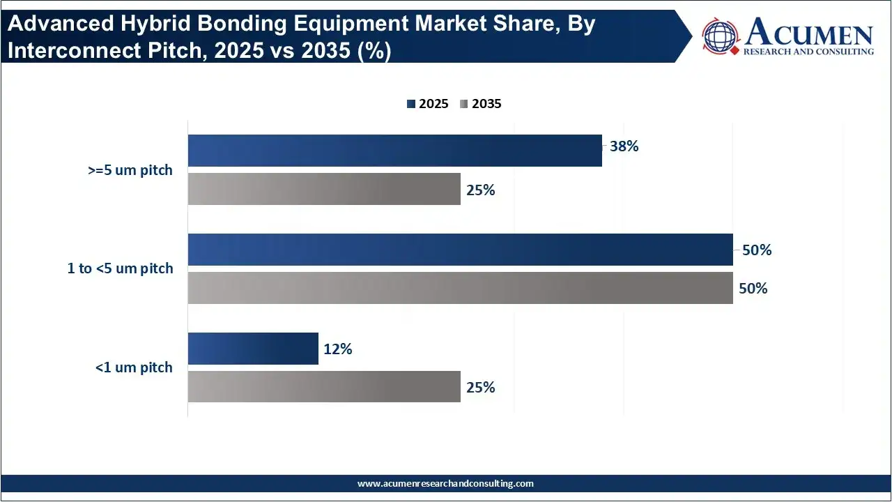
At Least 5 µm: This was the second-largest category in 2025, accounting for 38% of the market and generating USD 410.40 million. Revenue is expected to reach USD 1,897.21 million by 2035, registering a CAGR of 15.8%. Demand is supported by established applications that require reliable wafer-level and die-level connections without the most aggressive interconnect scaling.
End User Insights
IDMs and Memory Manufacturers: IDMs and memory manufacturers dominated the market in 2025, accounting for 58% of the total share and generating USD 626.40 million. Revenue is projected to reach USD 4,249.74 million by 2035 at a CAGR of 20.4%. Their leadership is supported by direct investments in advanced memory production, HBM manufacturing, and proprietary semiconductor integration technologies.
Foundries: Foundries represented the second-largest end-user category in 2025, accounting for 33% of the market and generating USD 356.40 million. The segment is expected to reach USD 2,352.53 million by 2035, registering a CAGR of 20.0%. Growing demand for advanced-node manufacturing, chiplet integration, and differentiated packaging solutions is supporting investment in hybrid bonding capabilities.
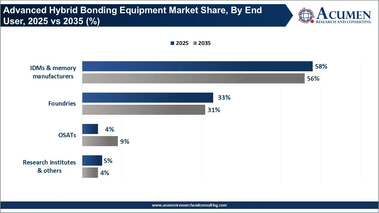
OSATs: OSATs are projected to be the fastest-growing end-user segment, registering a CAGR of 30.5% during 2026–2035. Their market share is expected to increase from 4% in 2025 to 9% by 2035, with revenue reaching USD 682.99 million. Growth is driven by expanding outsourced advanced packaging requirements and increasing investment in heterogeneous integration and high-density packaging services.
Wafer Size Insights
300 mm: The 300 mm wafer category dominated the market in 2025, accounting for 92% of the total share and generating USD 993.60 million in revenue. It is projected to reach USD 7,285.27 million by 2035 at a CAGR of 21.3%. Its dominance reflects the widespread use of 300 mm wafer infrastructure across advanced memory, logic, and high-volume semiconductor manufacturing.
Advanced Hybrid Bonding Equipment Market Share, By Wafer Size, 2025 & 2035 (%)
| Wafer Size | Revenue Share, 2025 (%) | Revenue Share, 2035 (%) |
|---|---|---|
| 300 mm | 92% | 96% |
| 200 mm & below | 8% | 4% |
200 mm and Below: This category accounted for 8% of the market in 2025, generating USD 86.40 million. Revenue is projected to reach USD 303.55 million by 2035 at a CAGR of 12.5%. Demand is supported by specialized applications, including sensors, MEMS, RF devices, and legacy semiconductor production. However, comparatively lower investment in new capacity limits its growth relative to 300 mm wafer processing.
Regional Insights
Asia Pacific to Sustain its Dominance by 2035
Asia-Pacific dominated the advanced hybrid bonding equipment market in 2025, accounting for 85% of the global market and generating revenue of USD 918.00 million. The regional market is projected to reach USD 5,995.17 million by 2035, registering a CAGR of 19.9% during 2026–2035. Despite its share declining to 79% by 2035, Asia-Pacific is expected to retain its leading position throughout the forecast period. Growth is primarily driven by the region's established semiconductor manufacturing ecosystem, expanding investments in advanced packaging, and increasing demand for high-bandwidth memory and 3D semiconductor integration.
Taiwan, South Korea, Japan, and China are important markets, supported by the presence of major foundries, memory manufacturers, and semiconductor equipment suppliers. Investments in HBM production, advanced logic manufacturing, 3D NAND, and chiplet-based architectures are increasing the need for precision bonding systems, surface preparation technologies, and advanced alignment and inspection equipment.
North America to Grow at the Rapid Pace During the Forecast Period
North America accounted for an 11.0% share of the advanced hybrid bonding equipment market in 2025, generating USD 118.80 million in revenue. The region is projected to register the fastest growth, with a CAGR of 25.3% from 2026 to 2035, reaching USD 1,214.21 million by 2035. Growth is supported by increasing investments in domestic semiconductor manufacturing, advanced packaging infrastructure, and AI-focused chip production. The United States represents the primary regional demand center, driven by investments from companies such as Intel, TSMC, and other semiconductor manufacturers expanding their advanced manufacturing capabilities.
Government-backed semiconductor initiatives are also supporting domestic production capacity, research facilities, and advanced packaging technology development. Equipment suppliers, including Applied Materials, Onto Innovation, and KLA, contribute to the regional ecosystem through semiconductor process engineering, inspection, and metrology capabilities.
Country-level Competitive and Investment Opportunities:
| Country | Competitive landscape | Investment and business opportunities |
|---|---|---|
| United States | Applied Materials, Intel, KLA, Onto Innovation, and TSMC are important participants in the semiconductor and advanced packaging ecosystem. | Opportunities in die-to-wafer bonding systems, advanced metrology, wafer preparation, integrated packaging equipment, and domestic equipment R&D. |
| Taiwan | TSMC, ASE Technology Holding, SPIL, and major international equipment suppliers support the country's advanced packaging ecosystem. | Opportunities in HBM-related packaging, wafer-to-wafer bonding, precision alignment, automated inspection, and advanced packaging production-line expansion. |
| South Korea | Samsung Electronics, SK hynix, Hanmi Semiconductor, and major semiconductor equipment suppliers are central to the ecosystem. | Opportunities in memory stacking, HBM packaging, fine-pitch bonding, die-to-wafer equipment, and advanced manufacturing process development. |
| Japan | Tokyo Electron, SCREEN Holdings, Canon, Nikon, Shibaura Mechatronics, and Kioxia contribute to the semiconductor manufacturing ecosystem. | Opportunities in precision alignment, wafer cleaning, surface preparation, inspection, advanced materials, and semiconductor equipment localization. |
Competitive Landscape
- BE Semiconductor Industries (BESI): A major hybrid bonding equipment supplier developing die-to-wafer bonding systems, including its Kinex platform, for advanced semiconductor packaging and 3D integration.
- Applied Materials: Develops materials engineering, wafer processing, planarization, and inspection technologies while collaborating with BESI on integrated hybrid bonding solutions.
- EV Group (EVG): Provides wafer bonding, surface preparation, and precision alignment technologies supporting wafer-to-wafer bonding and advanced 3D integration.
- SUSS MicroTec: Supplies wafer bonding, temporary bonding, lithography, and related process equipment used in advanced semiconductor packaging applications.
- ASMPT: Develops semiconductor assembly and advanced packaging technologies, including precision placement and interconnection solutions for heterogeneous integration.
- Tokyo Electron: Contributes to the semiconductor manufacturing ecosystem through wafer cleaning, deposition, coating, and other process technologies relevant to hybrid bonding preparation.
- SCREEN Holdings: Supplies wafer cleaning and surface preparation systems that support contamination control and surface quality requirements in advanced bonding processes.
- Onto Innovation: Provides inspection, metrology, and process control technologies that help semiconductor manufacturers monitor defects, overlay accuracy, and packaging quality.
- KLA Corporation: Supports advanced semiconductor manufacturing through defect inspection, process control, and metrology solutions essential for maintaining bonding quality and production yields.
- Lam Research: Provides wafer fabrication and materials processing technologies that support surface engineering and process requirements in advanced semiconductor integration.
- Kulicke & Soffa: Develops advanced packaging, die bonding, and semiconductor assembly solutions relevant to next-generation interconnect and heterogeneous integration requirements.
- Hanmi Semiconductor: Supplies advanced packaging equipment, including thermal compression bonding systems, supporting HBM manufacturing and memory packaging requirements.
- Nikon Corporation: Contributes precision optical, alignment, and semiconductor lithography technologies that support advanced manufacturing accuracy and wafer-level integration.
- Canon Inc.: Provides semiconductor lithography, nanoimprint, and precision manufacturing technologies relevant to advanced packaging and high-density semiconductor integration.
- Shibaura Mechatronics: Develops semiconductor manufacturing and packaging equipment, including wafer processing and bonding-related technologies for advanced semiconductor production.
Strategic Developments
- In October 2026, Applied Materials and BE Semiconductor Industries expanded their strategic collaboration to accelerate next-generation advanced packaging technologies for AI infrastructure. Under the expanded partnership, BESI joined Applied Materials' EPIC Center as an Innovation Partner.
- In September 2026, Tata Electronics and BE Semiconductor Industries entered into a strategic partnership to strengthen India's advanced semiconductor packaging capabilities. The collaboration will support technology readiness at Tata Electronics' semiconductor packaging facility in Jagiroad, Assam, through BESI's advanced packaging equipment portfolio.
Segments Covered
By Bonding Approach
- Wafer-to-Wafer (W2W)
- Die-to-Wafer (D2W)
- Die-to-Die & Collective Die-to-Wafer
By Equipment Type
- Hybrid Bonding Systems (W2W & D2W Bonders)
- Surface Preparation & Activation (Plasma Activation, Cleaning, CMP for Bonding)
- Alignment, Metrology & Inspection
- Die Preparation & Handling (Dicing, Temporary Bonding/Debonding)
By Application
- Logic & 3D SoC / Chiplets (Including AI/HPC Processors)
- 3D NAND
- CMOS Image Sensors
- HBM & DRAM
- Others (Co-Packaged Optics, MicroLED, RF/MEMS)
By Interconnect Pitch
- >=5 um pitch
- 1 to <5 um pitch
- <1 um pitch
By End User
- IDMs & memory manufacturers
- Foundries
- OSATs
- Research institutes & others
By Wafer Size
- 300 mm
- 200 mm & below
By Region
- North America
- Europe
- Asia-Pacific
- Latin America
- Middle East & Africa
Looking for discounts, bulk pricing, or custom solutions? Contact us today at sales@acumenresearchandconsulting.com
Frequently Asked Questions

Related Market Research Reports
August 2026
December 2025
October 2024
February 2023
December 2025
March 2024
October 2022
June 2026