
Semiconductor Inspection Systems Market Size, Share, Trends, Report 2026 To 2035
Semiconductor Inspection Systems Market (By Inspection System Type: Wafer Inspection Systems, Mask & Reticle Inspection Systems, Package Inspection Systems, Others; By Technology: Optical-based, Electron beam-based, X-ray-based, Ion beam, Hybrid / multi-modal, Others; By Wafer Size: 300 mm, 200 mm, ≤150 mm, Other/non-wafer; By End User: Pure-play foundries, Memory manufacturers, Other IDMs, OSATs, Others; By Manufacturing Application: Wafer / Device Manufacturing, Mask & Reticle / Lithography, Advanced packaging, Package / Final Inspection, Others) - Global Industry Analysis, Size, Share, Growth, Regional Analysis, Trends and Forecast 2026 - 2035
- Last Updated: 18 Aug 2026
- Report Code: ARC3964
- Category: Semiconductor and Electronics
Semiconductor Inspection Systems Market Size and Forecast Report 2026 To 2035
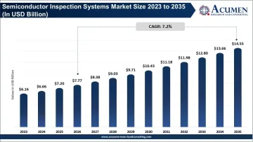
The global semiconductor inspection systems market size was valued at USD 7.20 billion in 2025. The market is seen to reach at USD 14.55 billion by 2035, while promising a growth at CAGR of 7.2% during the forecast period of 2026-2035.
Report Highlights
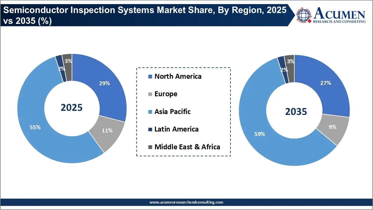
- By region, Asia Pacific dominated the semiconductor inspection systems market with a 55% share in 2025, supported by the concentration of advanced foundries, memory manufacturers, IDMs, advanced packaging facilities, and large-scale semiconductor equipment investments across Taiwan, South Korea, China, and Japan.
- By region, North America accounted for 29% of the semiconductor inspection systems market in 2025, with the regional market projected to grow from approximately $2.25 billion in 2026 to $3.93 billion by 2035, representing a 6.4% CAGR.
- By region, Middle East & Africa accounted for 3% of the market in 2025, with the regional market expected to increase from approximately $0.23 billion in 2026 to $0.44 billion by 2035, representing a 7.2% CAGR.
- By inspection system type, wafer inspection systems held the largest market share of 54% in 2025, driven by the increasing need to identify particles, pattern defects, scratches, contamination, and process-induced abnormalities across high-volume semiconductor manufacturing.
- By inspection system type, mask and reticle inspection systems accounted for the second-largest share of 20% in 2025, supported by increasingly complex lithography patterns and the need to maintain photomask quality as advanced and EUV-based manufacturing expands.
- By technology, optical-based inspection accounted for the largest 58% share in 2025, owing to its high-throughput capabilities and suitability for monitoring large wafer surfaces across high-volume fab operations.
- By technology, electron beam-based inspection held the second-largest share of 32% in 2025, supported by its higher resolution and growing importance in advanced-node manufacturing involving GAA transistors, advanced DRAM, 3D NAND, and increasingly complex device geometries.
- By wafer size, 300 mm wafers dominated the market with a 67% share in 2025, and their share is projected to increase to 71% by 2035, supported by continued investment in advanced logic, memory, AI processors, high-performance computing, and high-volume semiconductor production.
- By wafer size, 200 mm wafers represented the second-largest segment with a 23% share in 2025, supported by continued demand from mature-node applications such as automotive semiconductors, power devices, analog chips, MEMS, sensors, and industrial electronics.
- By end user, pure-play foundries held the largest market share of 40% in 2025, reflecting their high-volume manufacturing operations and the need for inspection, metrology, defect review, and process monitoring across diverse chip production programs.
- By end user, memory manufacturers accounted for the second-largest share of 30% in 2025, driven by the need for highly repeatable manufacturing and increasingly sophisticated inspection requirements across DRAM, HBM, and 3D NAND production.
- By manufacturing application, wafer and device manufacturing dominated the market with a 67% share in 2025, as inspection is required throughout lithography, deposition, etching, implantation, cleaning, and pattern-forming processes where defects can directly affect wafer yield.
- By manufacturing application, mask and reticle/lithography inspection represented the second-largest share of 18% in 2025, reflecting the critical role of lithography in transferring increasingly complex circuit patterns onto wafers.
- South Korea was projected to spend approximately $21.5 billion on semiconductor equipment in 2025, with memory and advanced-logic expansion supporting demand for high-resolution defect inspection, e-beam systems, wafer inspection, and metrology technologies.
- India has more than 12 approved semiconductor manufacturing units with cumulative investment exceeding ₹1.64 lakh crore, creating an emerging market for wafer inspection, metrology, package inspection, and testing equipment as its semiconductor manufacturing and packaging ecosystem develops.
Semiconductor Inspection Systems Market Overview
The relevance of semiconductor inspection systems is growing in line with the miniaturization of process nodes, transistor density and memory configurations, along with more sophisticated packaging designs, and all will call for more investment from the silicon foundry as wafer volumes expand. The market for general semiconductor production equipment clearly shows this level of investment is being deployed, with overall semiconductor equipment billings around the world expected to increase to $135.1B (year-over-year up 15% in 2025) with Taiwan expected to more than double their investment to $31.5B (+90% year-over-year) as Korea gains 26% investment year-over-year at $25.8B and with China still showing the largest level of market investment with $49.3B in 2025.
As foundries investment in advanced-node logic, HBM, 3D NAND, and advanced packaging continues, inspection systems are proving to be indispensable in helping find defects, monitor process variations and maintain yields. SEMI predicts front-end fab equipment investment will approach $130B annually by 2026, an increase of 18% compared to 2025; that represents significant new capacity which will need a strong layer of inspection and process control technology.
How Much Are Semiconductor Manufacturers Investing in New fabs?
| Company/Country | Location/Project | Recent Investment |
|---|---|---|
| TSMC | United States, Arizona | $165 billion planned U.S. investment announced in March 2025, including three additional fabs, two advanced packaging facilities and an R&D center; the planned U.S. investment was subsequently reported at $265 billion in July 2026 |
| SK hynix | South Korea, Yongin and Cheongju | $38.3 billion newly approved investment through 2031 |
| Samsung | United States, Texas | Samsung's Austin and Taylor campuses generated $10.9 billion in economic impact in 2025 and supported 28,746 jobs; the Taylor expansion remains part of its broader U.S. semiconductor manufacturing build-out |
| TSMC + Sony | Japan, Kumamoto | $4.69 billion joint venture investment |
| Intel | United States, Arizona and Ohio | Intel's Ohio fab complex is projected to exceed $100 billion in total cost; the company also announced a $19.7 billion equity raise in August 2026 to support ongoing and future projects |
| South Korea semiconductor industry | Korea memory and logic fabs | $25.8 billion in semiconductor equipment spending in 2025, up 26% YoY |
| Japan semiconductor industry | Domestic advanced-node and specialty fabs | $9.5 billion in semiconductor equipment spending in 2025, up 22% YoY |
How are AI and Machine Learning Changing Semiconductor Inspection?
- AI is also driving defect detection and classification. Inspection systems are better at identifying real defects from spurious signals. Systems can classify defect types like particles, residues, scratches, pattern abnormalites with reduced human input.
- Analysis of high dimensional inspection images is made more effective with the use of deep learning. As current advanced nodes, complex pattern images are generated more frequently, making small, true defect signatures difficult to detect.
- The load placed on defect review is beginning to be eased. Optical inspection at advanced nodes often returns large amounts of potential defect candidates, so eBeam review relies on AI to filter and prioritize, though it can generate over 100 times more potential defect candidates for review compared to advanced and prior node requirements, as has been previously reported by Applied Materials.
- Applied Materials SEMVision H20 integrates eBeam imaging technology with deep learning that differentiates from actual defects and classifiers defect types using data that is constantly retrained from the chipmaker's fabrication.
Market Dynamics
Driver
Increasing Defect Complexity at Advanced Semiconductor Nodes
The push to smaller dimensions, 3D device structures and higher levels of integration is only exacerbating the growth of the number and nature of the defects that semiconductor manufacturers must identify, characterize and classify. Inspection systems are producing massive amounts of defect candidates that can’t all possibly be of concern, but it is often difficult to distinguish the process-yield impacting defects from non-critical signals.
Machine learning can automatically perform the job that human reviewers are trained to do-and would otherwise have to painstakingly conduct for potentially hundreds or thousands of candidates-differentiating the truly worrisome defects, prioritizing items needing review, correlating those anomalies to specific process conditions and ultimately reducing the hours needed for engineering disposition.
Applied Materials, for example, says advanced-node optical inspection can generate up to 100× more defect candidates for eBeam review, creating a strong need for automated AI-based classification.
Restraint
Difficulty Scaling AI Models from Laboratory Performance to High-volume Fabs
A major limitation is that strong AI accuracy in controlled datasets does not automatically translate into reliable high-volume manufacturing performance. A 2026 review found that although published semiconductor vision-inspection systems frequently report 98%–99% accuracy, only 17% of the reviewed studies reported full-scale high-production deployment, reflecting challenges around data quality, model robustness, changing process conditions and integration with existing fab infrastructure. In addition, semiconductor manufacturers need highly explainable and consistent results because false positives can increase review workloads while missed defects can directly affect yield and product reliability.
Opportunity
AI-enabled Closed-loop Inspection and Process Control
The largest opportunity lies in connecting inspection systems with metrology, equipment sensors and process-control platforms to create a more autonomous feedback loop. Instead of simply detecting a defect after a process has occurred, artificial intelligence (AI) can correlate inspection results with equipment and process data to identify emerging process drift and support faster corrective action.
Recent research into ML-enabled in-situ semiconductor diagnostics specifically highlights anomaly detection and predictive maintenance as pathways toward real-time decision-making. This creates an opportunity for inspection-system suppliers to expand from selling detection hardware toward AI-enabled process intelligence, defect analytics, automated review and closed-loop manufacturing solutions.
Regional Insights
How did Asia Pacific Become the Center of Semiconductor Inspection Demand?
Asia Pacific dominated 55% of the semiconductor inspection systems market in 2025 and expected to rise its share to 59 percent by 2035. Asia Pacific was expected to expand approximately $4.27 billion in 2026 to $8.58 billion by 2035 at a CAGR of 8.1%. The region holds dominance mainly on account of concentration of advanced semiconductors manufacturers foundaries, memories makers, integrated devices manufacturers, advanced packaging providers increasing its foundry and assembly space.
In 2025, SEMI forecasted china spending as high as approximately $38 billion on semiconductor manufacturing equipment and Taiwan spending of $21 billion on manufacturing equipment just shows the capacity of equipment procurement driven by chip makers.
The demand is also becoming more technologically intensive. Advanced logic, EUV lithography, 3D NAND, DRAM and advanced packaging require tighter control of critical dimensions, overlay, pattern defects and contamination, increasing the need for both high-throughput optical inspection and higher-resolution e-beam systems.
Top Asian Countries for Semiconductor Inspection Equipment Investment
| Country | Semiconductor Investment and Manufacturing Significance | Impact on Inspection Equipment Demand |
|---|---|---|
| Taiwan | Taiwan remains one of the world's most important advanced-foundry manufacturing centers. SEMI projected approximately $21 billion in semiconductor manufacturing equipment investment for Taiwan in 2025. | High concentration of advanced-node production creates strong demand for optical inspection, e-beam inspection, critical-dimension metrology, overlay measurement and mask/reticle inspection, particularly as fabs move toward increasingly complex process geometries. |
| South Korea | South Korea is a major memory and advanced-logic manufacturing hub, with approximately $21.5 billion in projected semiconductor equipment spending in 2025. | Samsung and SK hynix's expansion of DRAM, NAND and advanced logic manufacturing supports demand for high-resolution defect inspection, e-beam systems, wafer inspection and metrology, particularly for advanced memory structures and EUV-related processes. |
| China | China was expected to lead global semiconductor equipment investment in 2025 at approximately $38 billion, despite a projected decline from the previous year. | Capacity expansion across mature-node logic, power semiconductors, memory and other devices is generating substantial demand for inspection systems. Export restrictions on advanced equipment are also encouraging greater development and adoption of domestic inspection technologies, particularly for mature-node manufacturing. |
| Japan | Japan combines a large semiconductor manufacturing base with a strong domestic semiconductor-equipment ecosystem. New investments include the $4.69 billion TSMC–Sony Kumamoto project, which is targeting volume production by 2029. | Demand comes from image sensors, memory, automotive and specialty semiconductor manufacturing, while Japanese equipment suppliers also strengthen the country's position as an important inspection and metrology technology development and production center. |
| India | India is building a new semiconductor manufacturing and packaging ecosystem, with the government reporting 12 approved semiconductor manufacturing units and more than ₹1.64 lakh crore in cumulative investment. | New fabs and OSAT/ATMP facilities are creating an emerging requirement for wafer inspection, metrology, package inspection and testing equipment, although India's inspection demand remains smaller than the established Asian semiconductor hubs. |
North America Semiconductor Inspection Systems Market: Investment and Capacity Outlook
In 2025 North America accounted for a 29% share of the semiconductor inspection systems market but is expected to account for 27% by 2035. The regional market is predicted to grow from an estimated $2.25b in 2026 to $3.93b by 2035, reflecting a 6.4% CAGR.
This opportunity is highly linked to the growth in U.S. domestic semiconductor manufacturing capacity. New fabs and expansion projects boost the installed base of inspection equipment, whereas modernization efforts in existing factories generate upgrade and replacement demand for higher-resolution inspection, metrology, and automated defect-classification systems.
North America also possesses a concentration of semiconductor equipment and process control technology companies, making the region a prominent market not just as an equipment-consuming territory, but also as a technology-developing center.
Middle East & Africa Semiconductor Inspection Systems Market and Manufacturing Outlook
The Middle East & Africa accounted for 3% of the semiconductor inspection systems market in 2025. The regional market is expected to increase from approximately $0.23 billion in 2026 to $0.44 billion by 2035, representing a 7.2% CAGR.
The region is still at an earlier stage of semiconductor manufacturing development than Asia Pacific, North America and Europe, so demand is being shaped more by new electronics manufacturing capacity, semiconductor-related industrial development, testing activities and technology localization initiatives than by a large installed base of advanced fabs.
Saudi Arabia is becoming particularly relevant as it seeks to diversify its economy toward advanced technology and manufacturing under Vision 2030. Increasing digital infrastructure, data-center development and industrial automation can gradually strengthen semiconductor demand, while any future expansion of local semiconductor manufacturing or packaging would create additional requirements for inspection, testing and quality-control equipment.
Segmental Insights
Inspection System Type Insights
The wafer inspection systems segment dominated the semiconductor inspection systems market with a 54% share in 2025 and is expected to maintain a leading 53% share by 2035. It leads because wafer inspection is the bedrock of semiconductor manufacturing and manufacturers are increasingly inspecting wafers for particles, pattern defects, scratches, contamination and process induced abnormalities and other yield affecting variations.
Chip makers are migrating to even smaller process geometry and structures so the margin for error in manufacturing is continuously decreasing, thus requiring high speed, high resolution wafer inspection for high volume fabs.
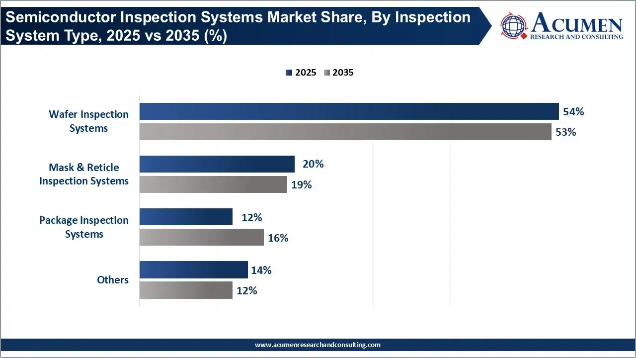
In 2025, mask and reticle inspection systems was the second-largest segment which held a share of 20%. They are an extremely critical segment as lithography becomes more stringent and wafer pattern fidelity depends on the photomask quality, while very small, complex patterns are being transferred to wafers and EUV lithography requires defect inspection at another level, which can be transferred across all wafers.
Technology Insights
Optical-based inspection technology dominated the market with a 58% share in 2025. The technology's share has been sustained and increased due to its advantages of providing high throughput inspection over the large wafer surface area while still maintaining a pace that can accommodate the high volume semiconductor manufacturing environment.
Optical methods are a ubiquitous element for particle, defect or process deviation inspection of a wafer during fabrication at virtually every processing step and have been the leading inspection methodology of choice throughout many wafer fab operations.
| Technology | Revenue Share, 2025 (%) |
|---|---|
| Optical-Based | 58% |
| Electron Beam-Based | 32% |
| X-Ray-Based | 4% |
| Ion Beam | 3% |
| Hybrid / Multi-Modal | 2% |
| Others | 1% |
Electron beam-based inspection captured the second largest market share in 2025 of 32% and will continue to be essential as semiconductor features shrink and require higher resolution defect inspection than optical-based systems can support. EBeam systems offer significantly higher resolution than optical systems and is ideal for advanced-node defect review, critical pattern analysis and the inspection of ultra-small features. With the increasing implementation of gate-all-around transistors, advanced DRAM, 3-D NAND and other complicated geometries, higher resolution inspection and review is a must.
Wafer Size Insights
The 300 mm wafer segment dominated the market with a 67% share in 2025 and is projected to increase its share to 71% by 2035, while revenue is expected to rise from approximately $5.21 billion in 2026 to $10.33 billion by 2035, representing a 7.9% CAGR.
The segment's dominance reflects the concentration of advanced logic, memory and high-performance semiconductor production on 300 mm wafers. Larger wafers enable manufacturers to produce more dies per wafer and improve manufacturing economics, making 300 mm platforms particularly attractive for high-volume production. The increasing construction and expansion of advanced fabs for AI processors, high-performance computing, smartphones and memory further strengthens the demand for 300 mm inspection systems.
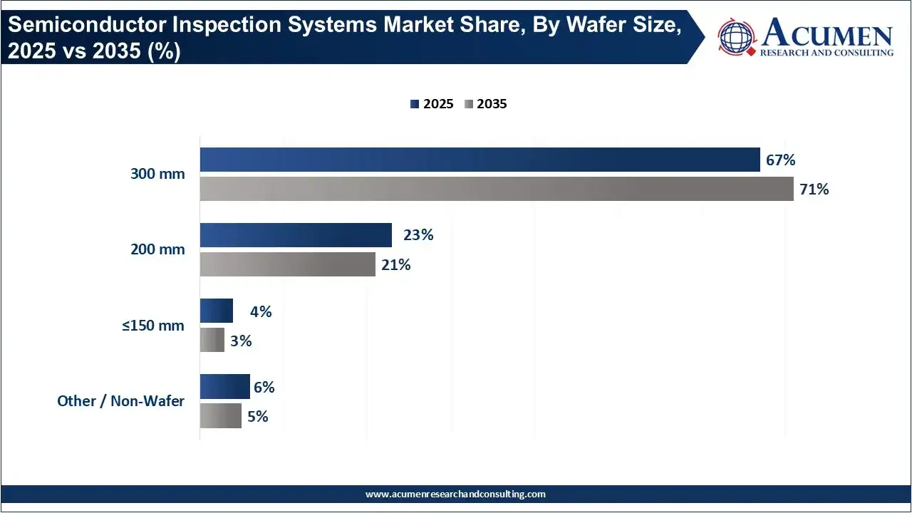
The 200 mm wafer segment held the second-largest share at 23% in 2025 and is projected to maintain a significant 21% share by 2035. Although 200 mm wafers are less dominant in leading-edge manufacturing, they remain strategically important for mature-node applications including automotive semiconductors, power devices, analog chips, MEMS, sensors and industrial electronics. Demand for these devices continues to expand because electrification, industrial automation, automotive electronics and IoT applications require large volumes of mature-node components.
End User Insights
With 40% market share in 2025 the foundries pure-play segment is expected to grow as the number of foundries increase. Leading role is often correlated with the nature of manufacturing in foundries; foundries produce semiconductors for many fabless semiconductor companies across varieties of product classes.
The rise of AI, HPC and advanced logic also elevate the priority for the front-end foundries, wherein any slightest variations will prove large consequences on yield and revenue, leading to increased demands for high-throughput optical inspection, high-resolution e-beam tools, metrology and automated defect-review solutions.
| End User | Revenue Share, 2025 (%) |
|---|---|
| Pure-Play Foundries | 40% |
| Memory Manufacturers | 30% |
| Other IDMs | 22% |
| OSATs / Advanced Packaging & Testing | 6% |
| Other Semiconductor Manufacturers | 2% |
The second largest end-user in 2025 is memory makers, with 30% revenue share. Memory makers must use repeatable and consistent manufacturing because they produce large number of similar structures across a vast wafer population. Inspection requirements also grows as manufactured complexity increases with DRAM, HBM, 3D NAND incorporating more layer counts, smaller feature size and more complicated structures.
Manufacturing Application Insights
Wafer and device manufacturing dominated the market with a 67% share in 2025. This segment consumes the largest amount of inspection solutions because there are a myriad of opportunities to introduce defects anywhere along the wafer processing flow including lithography, deposition, etching, implantation, cleaning, and pattern forming.
The growth of fab volumes driven by chips for AI, HPC and advanced memory will continue driving Wafer Level Inspection as the most important application for semiconductor inspection equipment in 2025.
| Manufacturing Application | Revenue Share, 2025 (%) |
|---|---|
| Wafer / Device Manufacturing | 67% |
| Mask & Reticle / Lithography | 18% |
| Advanced Packaging | 8% |
| Package / Final Inspection | 6% |
| Others | 1% |
Mask and reticle/lithography inspection accounted for 18% of the market in 2025 and represented the second most important application for semiconductor inspection in the manufacturing domain. Lithography is among the highest value-added of the critical stages in semiconductor production; circuit patterns are defined here that transfer and repeat on every individual wafer.
Semiconductor Inspection Systems Companies Across the Manufacturing
- KLA — A major process-control supplier spanning wafer inspection, defect review, metrology and data analytics, with a particularly strong position in optical inspection and advanced-node process control.
- Applied Materials — Provides optical and eBeam inspection and metrology technologies, including its PrimeVision, SEMVision and PROVision platforms, increasingly targeting advanced logic, HBM and advanced packaging.
- Hitachi High-Tech — Supplies CD-SEM, defect inspection and electron-beam technologies covering wafer measurement, defect detection and process monitoring across semiconductor manufacturing.
- Onto Innovation — Offers integrated 2D/3D inspection and metrology systems, including the Dragonfly G3, which combines multiple imaging modes, machine learning and 3D measurement for defect detection and yield improvement.
- Tokyo Electron — Provides semiconductor manufacturing equipment and process-control technologies used across deposition, etch, lithography and related production processes, supporting increasingly integrated fab-control workflows.
- SCREEN Semiconductor Solutions — Develops wafer-cleaning, inspection and semiconductor production technologies and serves high-volume semiconductor manufacturing environments.
- Lasertec — Specializes in high-precision inspection and metrology, particularly for photomasks and EUV-related semiconductor manufacturing, where defect detection and mask quality are critical to advanced-node production.
Major Product launches and Technology Developments
- April 2026 — Camtek announced the acquisition of Visual Layer. The acquisition is intended to strengthen Camtek's visual-AI capabilities by integrating Visual Layer's AI-based visual analytics into Camtek's inspection and metrology portfolio, showing how inspection suppliers are increasingly combining hardware with AI-driven analysis.
- January 2026 — Hitachi High-Tech launched FOUNDRY-MASTER Smart 2. The new optical emission spectrometer incorporates a scientific CMOS sensor and an ultra-stable spark source, reflecting the broader shift toward digitalized, high-precision analytical equipment for manufacturing quality control.
Segments Covered
By Inspection System Type
- Wafer Inspection Systems
- Mask & Reticle Inspection Systems
- Package Inspection Systems
- Others
By Technology
- Optical-based
- Electron beam-based
- X-ray-based
- Ion beam
- Hybrid / multi-modal
- Others
By Wafer Size
- 300 mm
- 200 mm
- ≤150 mm
- Other/non-wafer
By End User
- Pure-play foundries
- Memory manufacturers
- Other IDMs
- OSATs / advanced packaging & testing
- Other semiconductor manufacturers
By Manufacturing Application
- Wafer / Device Manufacturing
- Mask & Reticle / Lithography
- Advanced packaging
- Package / Final Inspection
- Other
By Region
- North America
- Europe
- Asia Pacific
- Latin America
- Middle East & Africa
Looking for discounts, bulk pricing, or custom solutions? Contact us today at sales@acumenresearchandconsulting.com
Frequently Asked Questions

Related Market Research Reports
August 2026
August 2026
August 2026
December 2025
July 2024
December 2023
August 2023
June 2023