
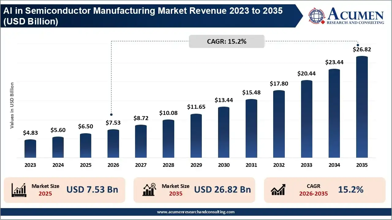
AI in Semiconductor Manufacturing Market Size to Hit USD 26.82 Billion by 2035, Reflecting CAGR of 15.2%
Published : 21 Aug 2026
Author : Simone Lamb



What is the AI in Semiconductor Manufacturing Market Size?
The global AI in semiconductor manufacturing market size was estimated at USD 6.50 billion in 2025 and is projected to hit USD 26.82 billion by 2035 growing at a CAGR of 15.2% during the forecast period of 2026-2035. The AI in semiconductor manufacturing market is expanding as semiconductor manufacturers increasingly integrate artificial intelligence and machine learning across fabrication, inspection, metrology, process control, equipment maintenance, yield management and advanced packaging.
Future Outlook
The future of AI in semiconductor manufacturing is expected to shift from individual AI-enabled inspection tools toward AI-driven, interconnected and increasingly autonomous fabs. As chipmakers move toward advanced process nodes, 3D architectures, high-bandwidth memory (HBM), chiplets and advanced packaging, the volume and complexity of manufacturing data will continue to increase.
- SEMI reported that global silicon wafer shipments increased 5.8% to 12,973 million square inches in 2025, with AI applications supporting demand for advanced epitaxial wafers and HBM-related polished wafers.
- Meanwhile, Applied Materials expects leading-edge foundry-logic, DRAM and advanced packaging to account for more than 80% of year-over-year growth in total wafer-fab equipment spending in 2026, highlighting the scale of investment being generated by AI-related semiconductor demand.
How Is AI Improving Wafer Inspection and Yield Management?
Al is changing wafer inspection, allowing manufacturers to take advantage of the massive volumes of inspection, metrology, equipment and process data produced during wafer fab. Novel AI and machine-learning models are able to detect process defects patterns, differentiate yield-killing defects from inspection noise and predict process excursioned or correlate defects to parameters virtually in real-time.
Applied Materials claims their ExtractAI technology can classify wafer-map signals after inspecting only 0.001 percent of wafer samples and their inspection approach cuts costs of essential defect capture by 3x. As many as 100 defects may be forwarded by optical to the e-beam inspection tool at advanced nodes, demanding an AI tool to aid in classification and prioritization.
Latest Trends
- AI agents are coming to semiconductor fabs: Instead of just using AI for individual inspection jobs, manufacturers are looking at using AI agents to examine process data; make repair recommendations; automate engineering tasks; and speed up decision-making. Siemens thinks agent-based AI, including industry-specific AI agents, is a coming trend in chipmaking.
- Machine-learning- based predictive maintenance is picking up: Chip manufacturers use ML algorithms to examine data from manufacturing equipment sensors and anticipate potential equipment failures to avoid costly downtime.
- Digital twins are moving into the center of the smart-fab: Semiconductor manufacturers are using digital twins and AI to model manufacturing flows, equipment, production environments, and manufacturing processes on a virtual platform to test changes before implementing them on a physical factory floor.
- AI is being deployed on edge devices: Semiconductor fabs can use edge-based architectures to examine sensor and inspection data close to the manufacturing equipment, instead of always uploading data to a centralized cloud for analysis. This enables lower latency monitoring of critical parameters and corrective actions.
- AI for inspection of wafers: Advanced semiconductor processes can lead to massive amounts of defect candidate data from automated inspection equipment. AI and ML help in categorizing and identifying critical defect patterns; minimizing false positives; and prioritizing data for humans.
Regional Outlook
Why Is Asia Pacific Expected to Maintain Its Leadership in the AI in Semiconductor Manufacturing Market Through 2035?
The Asia Pacific held the largest market share with 48.0% in the AI in semiconductor manufacturing market in 2025, which is predicted to extend up to 52.0% of the market share by 2035, and is expected to be the highest growing region registering highest regional CAGR at 16.2% over the forecast period from 2026 to 2035. The region leads with highest market share owing to its robust semiconductor manufacturing ecosystem; increased investments in advanced fabrication facilities, presence of leading foundries and semiconductor equipment manufacturers and rapid proliferation of artificial intelligence solutions across semiconductor design, manufacturing process optimization, defect detection, predictive maintenance and increasing yield rate in the fabrication process.
China, Taiwan, South Korea, and Japan play a significant role toward the revenue generation for this region by expanding semiconductor capacities, aided by government incentives and surging investments in advanced nodes and AI-assisted manufacturing capabilities. Increasing complexity of semiconductor manufacturing and to improve yield, decrease downtime, and optimize the allocation of resources are stimulating the adoption of AI by semiconductor manufacturers across the fab.
North America AI in Semiconductor Manufacturing Market Trends
North America held 28% of the AI in semiconductor manufacturing market share in 2025 and is expected to reach 25% by 2035. The market for this region is anticipated to grow at a CAGR of 13.7% between 2026 and 2035. Growing number of key semiconductor players, leading AI technology service providers, semiconductor manufacturing equipment developers, and research institutions is helping them maintaining robust position across the globe.
The U.S. is focusing on investing in U.S.-based manufacturing of semiconductors, advanced packaging, production of semiconductors integrated with AI chips, and smart manufacturing across the supply chain. However, the region's share is projected to decline moderately as Asia Pacific expands at a faster pace.
Who Are the Top Players Investing in the AI in Semiconductor Manufacturing Market?
| Company | Area of investment | Major AI/manufacturing development |
|---|---|---|
| Applied Materials | AI-enabled process control, inspection, metrology and manufacturing optimization | Its AIx platform analyzes millions of measurements across wafers and chips to identify process correlations and optimize semiconductor manufacturing recipes. |
| KLA Corporation | AI-powered inspection, metrology and yield management | KLA is expanding AI-driven process-control capabilities as increasing chip complexity and advanced packaging make yield management increasingly critical. Its FY2025 revenue reached $12.2 billion, up 24%. |
| ASML | AI-supported lithography and computational manufacturing | ASML is incorporating computational and software-based optimization into lithography workflows to improve process performance as semiconductor manufacturers move toward increasingly complex nodes. |
| Synopsys | AI-driven semiconductor design-to-manufacturing optimization | Synopsys is expanding AI capabilities across the semiconductor development workflow, connecting AI-driven design and analysis with manufacturing requirements to accelerate chip development. |
| Siemens | Industrial AI, digital twins and semiconductor manufacturing software | Siemens is applying industrial AI and digital-twin technologies to help semiconductor manufacturers optimize production processes, equipment performance and factory operations. |
| IBM | AI, semiconductor process optimization and advanced chip research | IBM has been developing AI-based approaches for semiconductor process development and materials discovery, supporting faster optimization of next-generation chip manufacturing technologies. |
| NVIDIA | AI computing infrastructure for semiconductor engineering | NVIDIA's accelerated-computing ecosystem enables semiconductor manufacturers and equipment companies to deploy AI models for simulation, inspection, digital twins and manufacturing optimization. |
| Intel | AI-enabled fabs and process manufacturing | Intel is integrating automation, data analytics and AI into its manufacturing operations as it expands advanced process technologies such as 18A and prepares future process nodes. |
| Samsung Electronics | AI-driven semiconductor manufacturing and yield optimization | Samsung is expanding AI-based manufacturing capabilities across semiconductor production, particularly for advanced logic and memory manufacturing where yield and process control are increasingly important. |
| TSMC | AI-enabled smart manufacturing and process control | TSMC is expanding smart-factory capabilities using AI, automation and data analytics to improve manufacturing efficiency, process control and yield across advanced-node fabs. |
Segments Covered
By AI Technology Architecture
- Classical Machine Learning
- Deep Learning
- Generative AI / Foundation Models
- Reinforcement Learning
- Other AI Technologies
By Offering
- Hardware
- Software / AI Platforms
- Services
By Deployment
- On-Premises / Fab-Local
- Cloud
- Hybrid
By Application
- Yield Optimization & Prediction
- Defect Detection & Classification
- Process Control & Optimization
- Predictive Maintenance & Equipment Health
- Manufacturing Planning & Scheduling
- Supply Chain & Inventory Optimization
- Others
By Manufacturing Stage
- Wafer Fabrication / Front-End Manufacturing
- Wafer Testing & Metrology
- Assembly & Packaging
- Final Testing
- Other
By End User
- Integrated Device Manufacturers (IDMs)
- Pure-Play Foundries
- OSATs / Semiconductor Packaging & Testing Companies
- Other Semiconductor Manufacturers
By Region
- North America
- Europe
- Asia Pacific
- Latin America
- Middle East & Africa (MEA)
Contact Us:
Mr. Richard Johnson
Acumen Research and Consulting
India: +91 8983225533