
Digital Twin in Semiconductor Market Size to Surge USD 41.82 Billion by 2035, Reflecting a CAGR of 36.2%
Published : 07 Sep 2026
Author : Raghuram Nair



What is the Digital Twin in Semiconductor Market Size?
The global digital twin in semiconductor market size was accounted for USD 1,900 million in 2025 and is projected to surge USD 41,827 million by 2035; growing at a CAGR of 36.2% during the forecast period from 2026 to 2035.
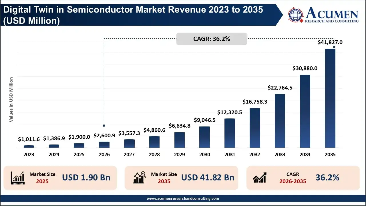
Digital Twin in Semiconductor Market Overview
The digital twin in semiconductor market is growing because manufacturers are using virtual representations of fabs, equipment, processes, products and the manufacturing environments to achieve greater efficiencies in manufacturing, higher yields, equipment throughput, and decision making. Digital twins use real-time data obtained from the equipment and processes, combine it with physics-based models, simulation technology, IoT connectivity, AI/ML, and data analytics to simulate and monitor semiconductor manufacturing worlds.
The technology is becoming particularly important as advanced-node manufacturing involves increasingly complex process flows, tighter process windows, higher equipment costs, and greater pressure to accelerate yield ramp-up. SEMI identifies digital twins as a key technology for the development of AI-driven autonomous semiconductor factories, with applications extending from individual tools and process sequences to entire production lines and fabs.
What Is Driving Digital Twin Adoption in Semiconductor Manufacturing?
- The increasing complexity of semiconductor manufacturing: The increasingly multi-step, intricately-coupled nature of advanced semiconductor manufacturing processes limits conventional experimentation. Identify the interactions and yield loss mechanisms requires analyzing enormous experimental design parameter spaces traditionally handled through physical testing.
- The increasing need for faster semiconductor yield optimization: By enabling manufacturers to use the simulation of various parameters and the predicted outcome of certain process variations, digital twins allow fewer physical wafer tests (reducing learning cycles) thereby accelerating yield optimization.
- Wafer experimentation being costly: Advanced materials and advanced process capabilities command a high price per wafer/fab-test time and there's an ongoing trend to move more process-development and optimization activities to virtual environments.
- Increased deployment of AI and machine learning in semiconductor manufacturing: AI/ML can analyze vast quantities of real-world and digital twin generated data to facilitate predictions, anomalies detection, optimal process adjustments, and predictive maintenance.
What Are the Biggest Challenges to Implementing Digital Twins in Semiconductor Fabs?
There are many obstacles to realizing digital twins in semiconductor fabs because the technology must fuse highlycomplex equipment, process, production, and facility data while also ensuring data accuracy, security, and real-time accuracy. One of the most significant obstacles is data interoperability. Semiconductor fabs use machines and software systems from a variety of vendors with variable formats, interfaces, and granularities in the data produced.
Older equipment is also a challenge, as much legacy equipment lacks the necessary sensors, connection, or standard interface interfaces that would allow it to produce the constant flow of data needed to drive the digital twins for the process. The unwillingness on the part of chip manufacturers and equipment vendors toshare propriety equipment-, process- and production data is a fourth obstacle due to concerns with intellectual property, secrecy, and competition.
Digital Twin Applications Across the Semiconductor Value Chain
| Semiconductor Value Chain Stage | Digital Twin Applications | Key Benefits |
|---|---|---|
| Chip design and architecture | Virtual design validation, performance simulation, power and thermal modeling, design optimization | Faster design iterations, reduced physical prototyping, improved manufacturability |
| EDA and verification | Digital design models, virtual verification, system-level simulation, design-for-manufacturing analysis | Earlier identification of design issues and reduced verification time |
| Wafer fabrication | Fab-level simulation, process optimization, WIP-flow modeling, production scheduling | Higher throughput, improved capacity utilization and shorter cycle times |
| Etching and deposition | Process-condition modeling, equipment-performance monitoring, recipe optimization | Better process consistency and reduced variability |
| Metrology and inspection | Virtual metrology, anomaly detection, defect prediction, data-driven process monitoring | Faster detection of process deviations and reduced inspection burden |
| Semiconductor equipment | Equipment digital twins, health monitoring, predictive maintenance, virtual commissioning | Higher equipment availability, reduced downtime and improved OEE |
| Assembly and packaging | Packaging-process simulation, die placement optimization, thermal and mechanical modeling | Improved package reliability, yield and manufacturing efficiency |
| Advanced packaging and 3D ICs | Thermal modeling, warpage prediction, stress analysis, interconnect reliability and heterogeneous-integration simulation | Better management of complex thermal, mechanical and electrical interactions |
Digital Twin in Semiconductor Market Regional Outlook
Asia Pacific led the market share with approximately 42.0% in 2025 as it held the largest regional market and is projected to register the highest CAGR of 37.9% between 2026 and 2035. Taiwan, South Korea, and China are the highest contributors to semiconductor fabrication capacity in the Asia Pacific region, followed by Japan, Singapore and other countries in that list.
The market's growth drivers include huge investment in advanced node fabs, memory production, semiconductor packaging, and chips relating to AI are driving increased sophistication and intricacy in semiconductor manufacturing, which is likely to create a growing demand for effective virtual simulation and advanced real-time optimization in the segment.
North America represented 28.0% of the digital twin in semiconductor market in 2025, with the regional market valued at approximately $532.0 million. The market increased to $728.3 million in 2026 and is projected to reach approximately $10,456.7 million by 2035, registering a CAGR of 34.5% during 2026–2035. The United States represents the primary contributor to regional demand, supported by semiconductor manufacturing expansion, advanced chip design, AI infrastructure, EDA software development, and the presence of major semiconductor equipment and technology companies. The region is also benefiting from government incentives aimed at strengthening domestic semiconductor production, which is encouraging manufacturers to incorporate digital technologies during fab construction, commissioning, and production ramp-up.
Which Countries Are Leading Semiconductor Digital Twin Adoption?
- United States: United States has been a pioneer of digital twin adoption in the semiconductor market owing to its solid R&D network, established AI framework, giant EDA and simulation software providers and the presence of government-supported programs on semiconductor manufacturing, as well as global semiconductor players like Intel, NVIDIA, Applied Materials, Lam Research, Synopsys, Cadence and Ansys on developing the AI empowered semiconductor designing and manufacturing system.
- Taiwan: The country leads on the uptake of digital twin adoption due to its dense semiconductor manufacturing centers and most importantly a leading company, TSMC, is investing in building a digital environment that facilitates smart-factory implementation, including development of AI solutions, smart factory techniques and automation capabilities of the current production line and on new productions through adoption of the latest simulation technologies to implement comprehensive digital manufacturing processes.
- South Korea: It has been a leading emerging market of digital twin adopting supported by top South Korean players like Samsung Electronics and SK Hynix especially for advanced memories and AI semiconductors, as well as the general manufacturing production, for equipment condition monitoring, process simulation, maintenance predictive and yields enhancement, or the smart-factory framework.
- Japan: Japan has a well-developed system covering equipment, materials, electronics, and production technology along with increase of investment on developing the new generations of semiconductor production, while the national government supported programs in developing high-tech production or a smart manufacturing framework can boost the adoption of simulation, digital twin, AI and industrial automation system on the industry.
Leading Players & Investors in the Digital Twin in Semiconductor Market
The major companies in the digital twin technology ecosystem comprise: NVIDIA Corporation, Siemens AG, Ansys Inc., Synopsys Inc., Cadence Design Systems Inc., Dassault Systèmes SE, PTC Inc., Rockwell Automation Inc., Schneider Electric SE, Honeywell International Inc., ABB Ltd., and Hexagon AB.
Whereas Autodesk Inc., IBM Corporation, Microsoft Corporation, Amazon Web Services, Inc., Google LLC, Intel Corporation, Taiwan Semiconductor Manufacturing Company Limited (TSMC), Samsung Electronics Co., Ltd., SK hynix Inc., Micron Technology, Inc., GlobalFoundries Inc. and Infineon Technologies AG; all of these players are undertaking Digitaltwin Development via software platforms, AI simulations, digital process modelling of semiconductor and IaaCS solutions, alliances, acquisitions and investments.
Segments Covered in the Report
By Component
- Software
- Services
By Digital Twin Type
- Product
- Equipment/Asset
- Process
- Fab/System
- Supply Chain
By Deployment Mode
- On-Premises
- Cloud
- Hybrid
By Fab Type
- Front-End
- Back-End
- Other
By End User
- Foundries
- IDMs
- Fabless
- OSAT
- Equipment OEMs
- EDA/Software
- Research Institutes
- Other
By Region
- North America
- Europe
- Asia-Pacific
- Latin America
- Middle East & Africa
Contact Us:
Mr. Richard Johnson
Acumen Research and Consulting
India: +91 8983225533