
Semiconductor Inspection Systems Market Size to Reach USD 14.55 Billion by 2035 | CAGR of 7.2%
Published : 26 Aug 2026
Author : Simone Lamb



What is the Semiconductor Inspection Systems Market Size?
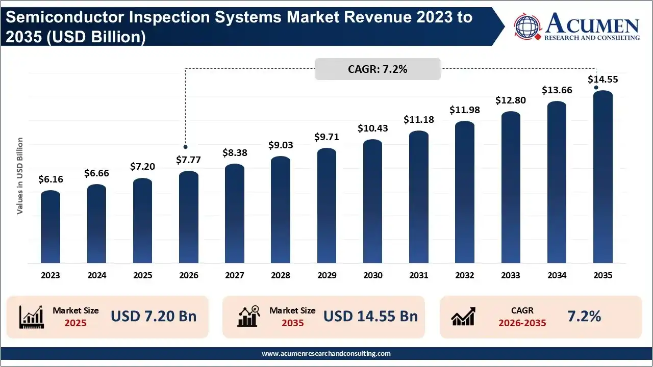
The global semiconductor inspection systems market size is expanding from USD 7.20 billion in 2025 to USD 14.55 billion by 2035 and market is growing at a CAGR of 7.2% over the forecast period from 2026 to 2035. As manufacturers transition toward 2 nm and below process nodes, gate-all-around (GAA) transistors, high-bandwidth memory (HBM), chiplets, and 2.5D/3D advanced packaging, the tolerance for manufacturing defects continues to decline. Smaller critical dimensions and increasingly complex structures require more precise and frequent inspection at multiple stages of production to identify defects before they affect yield.
What is Semiconductor Inspection Systems Market?
The semiconductor inspection systems market includes a broad range of equipment, technologies, software solutions, and integrated systems used to detect, classify, measure, and analyze defects and process variations in semiconductor device manufacturing. The market refers to systems that perform visual or other inspection techniques across semiconductor components such as wafers, masks, reticles, devices and other parts.
Technologies within this market can encompass a range of solutions, from classic optical inspection techniques to high-resolution electron-beam inspection, the analysis of large, complex patterned masks/reticles, wafer and substrate inspection systems, and advanced integrated inspection solutions in packaging (e.g., advance packaging inspection). Market analysis also often breaks down and includes the software applications with AI and advanced analytics for defect classification and root-cause analysis.
Future Outlook for the Semiconductor Inspection Systems Market
- AI-enabled inspection will become increasingly important as semiconductor manufacturers generate larger volumes of wafer and process data and require faster defect classification and root-cause analysis.
- Advanced-node manufacturing will increase inspection intensity, particularly as chipmakers move toward 2 nm and below processes, GAA architectures, and increasingly complex device structures.
- HBM and advanced packaging will become major growth areas for inspection systems as chiplets, 2.5D/3D integration, hybrid bonding, and stacked memory create new defect and alignment challenges.
- E-beam inspection is expected to gain importance for applications where conventional optical systems cannot provide sufficient sensitivity for extremely small defects.
- High-throughput optical inspection will remain essential because manufacturers need to inspect large wafer volumes without significantly increasing production cycle times.
- Inspection and metrology will become more integrated with process control, allowing manufacturers to connect defect information with equipment and process parameters for faster corrective action.
- Autonomous and closed-loop inspection systems will emerge, using AI to identify anomalies, determine their potential impact on yield, and support automated process adjustments.
Recent Product Launches and Strategic Developments
| Company | Product / Strategic Development | Significance |
|---|---|---|
| Onto Innovation | Dragonfly G5 Inspection System | Introduced for high-bandwidth memory manufacturing, including applications supporting HBM4 ramp-up and high-volume inspection. |
| Applied Materials | New wafer inspection and metrology technologies | Expanded inspection and metrology capabilities with AI-enabled defect analytics targeting advanced semiconductor manufacturing. |
| KLA Corporation | Advanced process-control solutions | Expanded process-control capabilities for next-generation semiconductor manufacturing and advanced packaging applications. |
| Applied Materials | New eBeam metrology and inspection systems | Introduced systems targeting DRAM and advanced packaging, addressing increasingly small defects in HBM and complex semiconductor structures. |
| Onto Innovation | Dragonfly G5 qualification for 2.5D AI packaging | Qualified its Dragonfly G5 system for applications in 2.5D AI packaging, strengthening its position in advanced packaging inspection. |
| Applied Materials & Advantest | EPIC platform collaboration | Announced collaboration to connect process development, metrology, inspection, and semiconductor testing to optimize end-to-end production workflows. |
Regional Analysis
Why Does Asia Pacific Dominate the Global Semiconductor Inspection Systems Market?
Asia Pacific was the leading semiconductor inspection systems market in 2025 with a share of 55%. The region holds vast share of the world's leading foundries, memory manufacturers, integrated device manufacturers (IDMs), and advanced packaging service providers. Countries like Taiwan, South Korea, China and Japan continue to be a major manufacturing hub for semiconductors, receiving massive investment across new fabrication capacity, newer process nodes, HBM, 3D NAND, and advanced packaging technologies.
Furthermore, with the advancement of complexity within semiconductor layers and structures, the requirement for high precision wafer inspection, mask inspection, and packaging inspection systems to check micro-level defects have started to gain more traction.
The domestic semiconductor manufacturing policy along with increased investments in artificial intelligence and high-performance computer chips has helped the manufacturers to increasingly opt for solutions like advanced optical inspection, e-beam inspection, and artificial intelligence based defect classification systems.
China Semiconductor Inspection Systems Market Analysis
- Among individual market regions in the world, China is one of the fastest growing important semiconductor inspection systems market due to the fast ramp-up of domestic wafer fab capacity, drive for semiconductor self-sufficiency in addition to heavy investment in advanced logic, memory and packaging technologies.
- New and expanding Chinese fabs at critical semiconductor clusters in Shanghai, Beijing, Shenzhen, Hefei, and Chengdu will drive increased Chinese demand for both optical and e-beam wafer inspection, defect review, and metrology in the near future as Chinese vendors expand advanced processor, memory chip and AI related semiconductor production to satisfy the domestic demand.
- China’s domestic semiconductor localization will further reshape domestic inspection equipment market in China. The high end segment continues to heavily rely on non-China vendors mainly for advanced node chips.
- Local players have been slowly gaining share in the mature nodes inspection market. Current estimations have domestic inspection system vendors contributing to less than 10% of the Chinese semiconductor inspection systems market value, primarily through products at mature nodes and related applications.
How Is North America's Semiconductor Manufacturing Expansion Driving Inspection Systems Demand?
North America accounted for 29% of the Semiconductor Inspection Systems Market in 2025, with the regional market projected to grow from approximately USD 2.25 billion in 2026 to USD 3.93 billion by 2035, registering a 6.4% CAGR during 2026–2035. The region's strong market position is primarily supported by the United States, which has been increasing domestic semiconductor manufacturing capacity through government incentives, private-sector investments, and the construction and expansion of advanced fabrication facilities. New fabs require sophisticated inspection systems to maintain process control and achieve high yields, particularly for advanced logic, memory, and AI-related semiconductor production.
United States Semiconductor Inspection Systems Market Analysis
- The United States has been the largest market for semiconductor inspection solutions and its growing semiconductor manufacturing footprint and expanded advanced packaging production capability via the CHIPS and Science Act is enhancing this market size.
- New and expanded fabs across Arizona, Ohio, Texas and New York will further build out capacity for wafer inspection, defect inspection and defect detection, metrology and process control systems at the process flows both for fab qualification and high-volume manufacturing.
- Growing demand for AI chips, advanced processors, memory, and HPC devices is also creating robust opportunity in the US market for wafer inspection systems.
- As device designers move to the industry’s most advanced process nodes and complex heterogeneous integration techniques, inspection equipment is required to effectively detect the tiniest defects, measure process variations, and prevent yield loss.
- Optical inspection is still the workhorse in high-speed production; however, e-beam inspection and other advanced wafer inspection solutions are becoming increasingly critical to address smaller defects, as well as advance package substrates.
Top Companies in the Semiconductor Inspection Systems Market
There is heavy competition in the semiconductor inspection systems market from well-established semiconductor equipment and process-control technology suppliers such as KLA Corporation, Applied Materials, ASML, Onto Innovation, Hitachi High-Tech, Lam Research, Nova Ltd., Thermo Fisher Scientific, SCREEN Semiconductor Solutions, and ZEISS.
These semiconductor companies are focusing on optical inspection, e-beam inspection, metrology, defect classification, AI-powered analytics, advanced packaging inspection, and high-resolution process control technologies that comply with advancing semiconductor industry needs. While KLA Corporation and Applied Materials have wide product ranges in inspection and process control products and solutions, Onto Innovation and Nova have a major foothold in certain critical inspection and metrology segments.
ASML and ZEISS play key roles for integrated lithography and semiconductor manufacturing technologies respectively. Hitachi High-Tech, Lam Research, Thermo Fisher Scientific and SCREEN Semiconductor Solutions are providing other pertinent inspection and measurement and process solutions.
Segments Covered
By Inspection System Type
- Wafer Inspection Systems
- Mask & Reticle Inspection Systems
- Package Inspection Systems
- Others
By Technology
- Optical-based
- Electron beam-based
- X-ray-based
- Ion beam
- Hybrid / multi-modal
- Others
By Wafer Size
- 300 mm
- 200 mm
- ≤150 mm
- Other/non-wafer
By End User
- Pure-play foundries
- Memory manufacturers
- Other IDMs
- OSATs / advanced packaging & testing
- Other semiconductor manufacturers
By Manufacturing Application
- Wafer / Device Manufacturing
- Mask & Reticle / Lithography
- Advanced packaging
- Package / Final Inspection
- Other
By Region
- North America
- Europe
- Asia Pacific
- Latin America
- Middle East & Africa
Contact Us:
Mr. Richard Johnson
Acumen Research and Consulting
India: +91 8983225533