
Semiconductor Process Control Equipment Market Size to hit USD 25.98 Billion by 2035
Published : 24 Aug 2026
Author : Raghuram Nair



What is the Semiconductor Process Control Equipment Market Size?
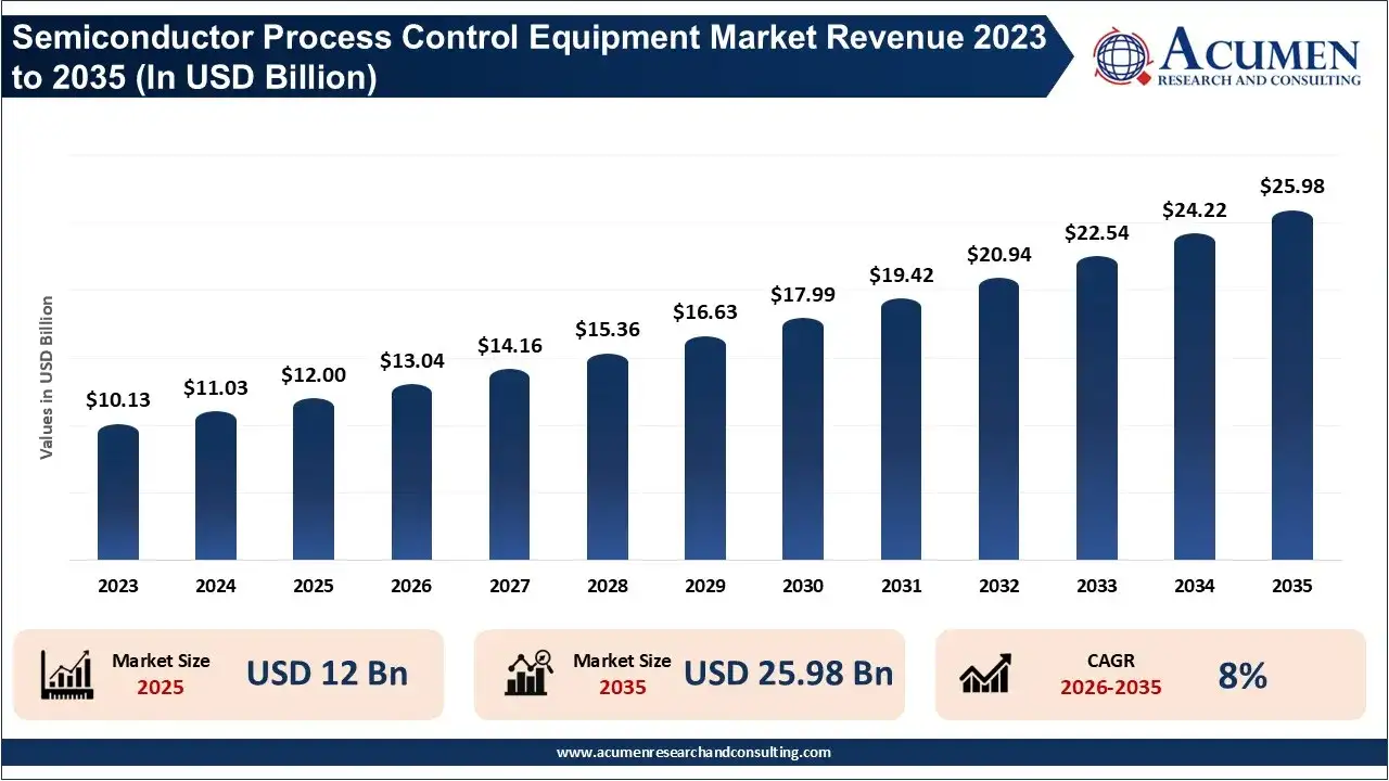
The global semiconductor process control equipment market is expected to hit $25.98 billion by 2035—up from $12 billion in 2025—driven by a steady compound annual growth rate (CAGR) of 8% over the forecast period from 2026 to 2035.
Why Is Asia Pacific Expected to Strengthen Its Leadership in the Semiconductor Process Control Equipment Market?
The market share was driven by Asia-Pacific in 2025 at 45%, expected to rise to 48% in 2035. The dominance of the region can be attributed to having the majority of major semiconductor manufacturing sites in the form of Taiwan, South Korea, China, and Japan and continued investment into state-of-the-art fabrication plants and new-generation technologies.
The growth in the market for sub-7 nm technology and the demand for AI chips, HBM as well as the demand for an increase in advance packaging technology would require the need for more equipment in the form of inspection, metrology and monitoring technology.
Why Will North America Remain a Major Market for Semiconductor Process Control Equipment Through 2035?
In 2025, North America generated around 28.5% of semiconductor process control equipment market revenue, showing a 7.3% CAGR during the forecast period. The region's prominent status can be attributed to the presence of major semiconductor manufacturers, equipment manufacturers, chip design companies, technology firms including those that are U.S.-based.
Furthermore, higher investment in in-house semiconductor manufacturing across North America through policies and legislation such as the CHIPS and Science Act is contributing to the growing demand of superior inspection and metrology tools for new and refurbish fabs. The expanding fabrication of new AI accelerators, ultra-advanced processors, memory based equipment and chips and those driven by HPC chips is increasing the dependency of sophisticated semiconductor process control.
How Is Semiconductor Manufacturing Expansion Creating Opportunities in the Middle East & Africa?
Middle East & Africa garnered a share of 6% of the semiconductor process control equipment market share in 2025, and the share is likely to remain similar during the forecast years for 2025-2035, as the market is estimated to register a CAGR of 8% between 2026 and 2035. Middle East & Africa’s semiconductor process control equipment market is driven by rising investments in electronics, electronics manufacturing services, semiconductor infrastructure, data centers and tech diversification across GCC economies.
Even though Middle East & Africa lags considerably behind Asia Pacific, Europe and North America in its current semiconductor manufacturing capacity, the rising spending on high-end electronic equipment, infrastructure on AI and tech-parks could drive growth opportunities over the foreseeable future with increasing demand for process metrology, process control equipment and quality inspection.
Government Initiatives Supporting Semiconductor Manufacturing
- United States' Chips and Science Act: U.S. CHIPS initiatives focus on domestic chip manufacturing, R&D and work-force development Increased fabrication capacity within US borders would drive the demand for inspection, metrology and process-control equipment, in particular for the leading-edge logic and memory sectors.
- European Union's European Chips Act: The European Chips Act provides for a comprehensive framework to bolster Europe's chip ecosystem, boost investment in manufacturing, R&D, advanced tech, as well as supply-chain robustness, with Europe's increased participation in global chip production, and the drive for production and process-control tech to ramp up.
- India Semiconductor Mission (ISM): The ISM in India sets to put in place a robust chip and display ecosystem, enabling India a manufacturing/design destination on the global chip/electronics scale and will push support for fab, display fabs, compound semiconductors, packaging and related eco systems in an array of new business for equipment suppliers.
Recent Product Launches and Strategic Developments
| Company | Product / Development | Key significance for semiconductor process control |
|---|---|---|
| Onto Innovation | Dragonfly G5 Inspection System | Launched for high-bandwidth memory (HBM) manufacturing, with a leading HBM manufacturer selecting the system for 2D inspection during HBM4 ramp-up Onto also received double-digit orders for Dragonfly G5 and 3Di technologies. |
| Applied Materials | New eBeam Metrology & Inspection Systems | Introduced new eBeam systems targeting DRAM and advanced packaging, addressing increasingly small features and defects in HBM and advanced semiconductor packages |
| Applied Materials | Advanced Packaging Portfolio Expansion | Expanded its advanced-packaging portfolio through NEXX Systems' panel-level electrochemical deposition technology, supporting fine-pitch I/O and AI-chip packaging requirements. |
| Onto Innovation | Dragonfly G5 qualification for 25D AI packaging | Dragonfly G5 was qualified for applications in 25D AI packaging, strengthening Onto's inspection and metrology capabilities for advanced AI-chip packaging. |
| ASML & Tata Electronics | Strategic Semiconductor Manufacturing Partnership | ASML and Tata Electronics signed an MoU to support the establishment and ramp-up of Tata's planned 300 mm semiconductor fab in Dholera, Gujarat, including lithography solutions, training and R&D infrastructure. |
| Applied Materials & Advantest | EPIC Platform Partnership | Applied Materials and Advantest announced collaboration to optimize end-to-end semiconductor production flows, connecting process development, metrology, inspection and final device testing. |
What Is the Future of Semiconductor Process Control Equipment?
The trend toward real-time AI and automation within semiconductor manufacturing will drive growth of the semiconductor process control equipment market as chips move into 2 nm and beyond process nodes and incorporate GAA architectures, HBM, 3D NAND, chiplets and advanced packaging that demand precise control over defects, critical dimensions (CDs), overlay, films, and process variations.
For instance: In October 2025 Applied Materials announced PROVision 10 eBeam metrology with sub-nanometer resolution and up to 10x the speed of traditional tech in 3D IC’s and June 2026 with a suite of new eBeam metrology products tailored to advanced packaging, where a few defects can take out an entire HBM stack.
Which Top Companies are operating in the Semiconductor Process Control Equipment Market?
The semiconductor process control equipment market is a competitive market that features key technology providers including KLA Corporation, Applied Materials, ASML, Onto Innovation, Hitachi High-Tech, Lam Research, Nova Ltd., Thermo Fisher Scientific, SCREEN Semiconductor Solutions, and ZEISS.
These players are fortifying their market stance by expanding their investments in wafer inspection, metrology, defect inspection, process monitoring, advanced packaging inspection, and AI-enabled process control solutions.
KLA and Applied Materials offer strong, broad portfolios that address most aspects of process control, whereas Onto Innovation and Nova offer a strong focus on advanced metrology and inspection; ASML and ZEISS are primarily related to lithography and mask/process control. Screen Semiconductor Solutions, Thermo Fisher Scientific, and Lam Research continue to provide specific and essential equipment and process control technology to the semiconductor manufacturing ecosystem.
Segments Covered
By Equipment Type
- Inspection Systems
- Metrology Systems
- Defect Review & Analysis Systems
By Technology
- Optical-Based
- Electron Beam-Based
- X-Ray-Based
- Scanning Probe / AFM-Based
- Electrical / Sensor-Based
- Other
By Wafer Size
- 300 mm
- 200 mm
- ≤150 mm
- Other / Non-Wafer
By End User
- Pure-Play Foundries
- IDMs
- Memory Manufacturers
- OSATs / Advanced Packaging & Testing
- Other Semiconductor Manufacturers
By Manufacturing Application
- Front-End of the Line (FEOL)
- Middle-of-Line / MOL
- Back-End-of-Line / BEOL
- Advanced Packaging
- Wafer-Level Testing
- Final / Package Testing
- Other
By Deployment Configuration
- Inline / In-Situ
- Standalone / Offline
By Region
- North America
- Europe
- Asia-Pacific
- Latin America
- Middle East & Africa
Contact Us:
Mr. Richard Johnson
Acumen Research and Consulting
India: +91 8983225533